MicroprocessorUnit 112 min read
Microprocessors: Basics, Architecture & Evolution
Unit 1 of Microprocessor: Covers the definition of microprocessors, their evolution, internal architecture (ALU, CU, registers), system components (CPU, memory, I/O), bus types (data, address, control), and real-world applications in embedded systems and computers.
TAKEAWAYS:
- A microprocessor is a single-chip CPU with ALU, CU, and registers that executes instructions via fetch-decode-execute cycles.
- The von Neumann architecture (stored-program concept) is the foundation of modern microprocessors, using a single bus for data and instructions.
- Key components include the ALU (arithmetic/logic), CU (control unit), registers (temporary storage), and clock (synchronization).
- Buses (data, address, control) connect the CPU to memory and I/O devices, with multiplexing (e.g., 8086’s 20-bit address bus over 16 lines) enabling efficient design.
- Microprocessors evolved from 4-bit (e.g., Intel 4004) to 32/64-bit (e.g., 8086, 80286), with pipelining and segmentation improving performance.
- Real-world uses include eSewa’s payment processing (8051-based embedded systems), Khalti’s secure transactions (microcontroller-based encryption), and NTC’s billing systems (8086/80286-based legacy hardware).
1. What is a Microprocessor?
A microprocessor is an integrated circuit (IC) that contains the Central Processing Unit (CPU) of a computer. It performs arithmetic, logic, and control operations by executing instructions stored in memory. Unlike general-purpose CPUs (which require multiple chips), microprocessors integrate ALU (Arithmetic Logic Unit), CU (Control Unit), registers, and clock circuitry onto a single chip.
Key Features:
- Single-chip design: Reduces size, cost, and power consumption.
- Programmable: Executes instructions from memory (von Neumann architecture).
- Clock-driven: Operations synchronized by a clock signal (e.g., 1 MHz to 5 GHz).
- Register-based: Uses temporary storage (e.g., accumulator, program counter, stack pointer) for fast data access.
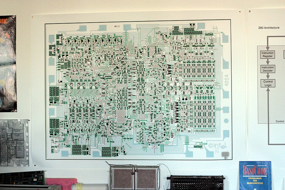 First commercial microprocessor (1971), 4-bit, 2300 transistors (Image: Wolfgang Stief from Tittmoning, Germany, CC0, via Wikimedia Commons)
(Note: The 4004 was used in calculators and early embedded systems, marking the start of microprocessor evolution.)
First commercial microprocessor (1971), 4-bit, 2300 transistors (Image: Wolfgang Stief from Tittmoning, Germany, CC0, via Wikimedia Commons)
(Note: The 4004 was used in calculators and early embedded systems, marking the start of microprocessor evolution.)
2. Von Neumann Architecture: The Foundation
All modern microprocessors follow the von Neumann architecture, proposed by John von Neumann in 1945. Its key principles:
- Stored-program concept: Instructions and data share the same memory.
- Single bus system: Data, instructions, and addresses travel over three buses:
- Data Bus (DB): Carries data/instructions between CPU, memory, and I/O (bidirectional).
- Address Bus (AB): Specifies memory/I/O locations (unidirectional, CPU → memory).
- Control Bus (CB): Carries signals like read/write, clock, interrupts (bidirectional).
How It Works: Fetch-Decode-Execute Cycle
Example: Loading a value from memory 2000H into the accumulator (8085):
- Fetch: PC (Program Counter) holds
2000H→ sent to MAR (Memory Address Register) → MDR (Memory Data Register) fetches data → IR (Instruction Register) stores it. - Decode: CU recognizes it as a load instruction (e.g.,
LDA 2000H). - Execute: Data moves to accumulator (ACC).
(Note: The diagram should show the three buses, MAR/MDR, and the fetch-decode-execute flow.)
3. Internal Architecture of a Microprocessor
A microprocessor’s core components:
| Component | Function | Example (8085) |
|---|---|---|
| ALU | Performs arithmetic (add, subtract) and logic (AND, OR) operations. | 8-bit ALU in 8085. |
| CU (Control Unit) | Decodes instructions and generates control signals. | Microprogrammed CU in 8085. |
| Registers | Temporary storage for data/instructions. | ACC, PC, SP, PSW (8085). |
| Clock | Synchronizes operations (e.g., 3 MHz in 8085). | Crystal oscillator. |
| Interrupt Logic | Handles external signals (e.g., keyboard input). | INTR, RST pins in 8085. |
Register Organization (8085 Example)
Real-World Tie-In:
- eSewa’s payment gateway uses an 8051-based microcontroller to process transactions. The ACC register handles encryption keys, while the PC register fetches instructions for validating user inputs.
4. Evolution of Microprocessors
Microprocessors evolved from 4-bit to 64-bit, with key milestones:
| Year | Microprocessor | Bit Width | Key Feature | Application |
|---|---|---|---|---|
| 1971 | Intel 4004 | 4-bit | First commercial microprocessor. | Calculators (Busicom). |
| 1974 | Intel 8080 | 8-bit | 8-bit ALU, 64KB address space. | Early PCs (Altair 8800). |
| 1978 | Intel 8085 | 8-bit | On-chip clock, interrupt logic. | Embedded systems (printers, toys). |
| 1979 | Intel 8086 | 16-bit | 16-bit registers, segmentation. | IBM PC (1981). |
| 1982 | Intel 80286 | 16-bit | Protected mode, 16MB address space. | Legacy servers. |
| 1985 | Intel 80386 | 32-bit | Pipelining, virtual memory. | Workstations. |
Why the Shift from 8-bit to 16-bit?
- 8-bit (8085): Limited to 64KB memory, slower for complex tasks.
- 16-bit (8086): Doubled data width → faster calculations (e.g., multimedia processing).
- Segmentation: 8086 used segment registers (CS, DS, SS, ES) to access 1MB memory via base + offset addressing.
Example: In NTC’s billing system, the 8086’s segmentation allows efficient access to customer records stored across multiple memory segments.
(Note: Highlight the 16-bit ALU, 16-bit registers, and segment registers.)
5. Buses: The Nervous System of a Microprocessor
Buses are the communication pathways between CPU, memory, and I/O. Three types:
| Bus Type | Direction | Width (8085) | Function |
|---|---|---|---|
| Data Bus | Bidirectional | 8-bit | Transfers data/instructions. |
| Address Bus | Unidirectional | 16-bit | Specifies memory/I/O location. |
| Control Bus | Bidirectional | Varies | Carries signals like READ, WRITE, RESET. |
Multiplexing in 8086
The 8086 has a 20-bit address bus but only 16 address lines (A0–A15). To address 1MB memory, it uses:
- A0–A15: Lower 16 bits of address.
- A16–A19: Multiplexed over AD0–AD7 (data bus) in time-division multiplexing.
- Segment registers (CS, DS): Provide upper 4 bits of the 20-bit address.
Example: To access memory location 1234:5678 (segment:offset):
- CS = 1234H, IP = 5678H.
- Physical address = (CS × 16) + IP = 12340H + 5678H = 179B8H.
(Note: Show the timing diagram where A0–A15 appear first, then AD0–AD7 carry data.)
6. Real-World Applications
1. eSewa (Payment Processing)
- Microprocessor Used: 8051-based microcontroller (8-bit).
- How It Works:
- The ACC register processes RSA encryption keys for secure transactions.
- The PC register fetches instructions to validate QR codes and OTP pins.
- Interrupts trigger when a user scans a QR code (via INTR pin).
2. Khalti (Mobile Banking)
- Microprocessor Used: ARM Cortex-M4 (32-bit, embedded in smartphones).
- How It Works:
- Pipelining speeds up AES encryption for transaction data.
- Segmentation (like 8086) manages user profiles and transaction logs in memory.
3. NTC’s Billing System (Legacy Hardware)
- Microprocessor Used: 8086/80286 (16-bit).
- How It Works:
- Segment registers map customer records (e.g.,
DS:2000Hfor user data). - DMA (Direct Memory Access) transfers bulk billing data to printers without CPU intervention.
- Segment registers map customer records (e.g.,
(Note: Label the ACC, PC, and interrupt pins.)
7. Exam Tip: What to Focus On
Based on past exam questions, prioritize these areas:
- Architecture Diagrams:
- Draw and label the 8085/8086 block diagrams (ALU, CU, registers, buses).
- Explain segmentation in 8086 (CS, DS, SS, ES registers).
- Bus Multiplexing:
- Describe how 8086 multiplexes address/data to save pins.
- Compare 8085 (dedicated buses) vs. 8086 (multiplexed).
- Fetch-Decode-Execute Cycle:
- Trace how an instruction (e.g.,
LDA 2000H) moves through MAR → MDR → ACC.
- Trace how an instruction (e.g.,
- Real-World Scenarios:
- Relate segmentation to NTC’s billing system or eSewa’s memory management.
- Explain DMA using Pathao’s ride-hailing data transfer (bulk GPS coordinates sent to servers without CPU delay).
- Common Pitfalls:
- Don’t confuse 8085 (8-bit) and 8086 (16-bit). Always mention segmentation for 8086.
- DMA is not an interrupt—it bypasses the CPU for high-speed transfers.
- Multiplexing saves pins but adds complexity (e.g., 8086’s AD bus).
Worked Example (Exam-Style Question):
Question: "Explain how the 8086 microprocessor accesses memory location 1234:5678. Draw a diagram showing the role of segment registers."
Answer:
- Physical Address Calculation:
CS = 1234H,IP = 5678H.- Physical address =
(CS × 16) + IP = 12340H + 5678H = 179B8H.
- Diagram:
- Bus Operation:
- A16–A19 (upper 4 bits) come from CS.
- A0–A15 (lower 16 bits) come from IP.
- AD0–AD15 multiplexes address first, then data.
Final Note:
- Memorize: 8085 vs. 8086 (bits, buses, segmentation).
- Draw: Block diagrams, bus multiplexing, fetch cycle.
- Apply: Relate to eSewa, Khalti, NTC in explanations.
- Avoid: Confusing DMA with interrupts or multiplexing with demultiplexing.
Based on the TU BSc CSIT syllabus for Microprocessor (CSC167), unit 1.
Discussion
Loading…