Computer ScienceNEB 2076 (old course)
What is Boolean algebra ? Describe AND and NAND gates with logic symbol, truth table and Venn diagram. [4+6]
10Answer
Boolean Algebra
Boolean algebra is a mathematical system that deals with binary variables having only two possible values, usually denoted 0 (false) and 1 (true). It was introduced by George Boole in 1854 to formalize logical reasoning. The algebraic structure consists of a set B = {0, 1} together with two binary operations – AND (·) and OR (+) – and a unary operation NOT ( ′ ), satisfying the following axioms:
| Axiom | Statement |
|---|---|
| Closure | 0 · 1, 0 + 1 ∈ B |
| Commutativity | A · B = B · A ; A + B = B + A |
| Associativity | (A · B) · C = A · (B · C) ; (A + B) + C = A + (B + C) |
| Distributivity | A · (B + C) = (A · B) + (A · C) ; A + (B · C) = (A + B) · (A + C) |
| Identity elements | A · 1 = A ; A + 0 = A |
| Complement | A · A′ = 0 ; A + A′ = 1 |
These rules allow any logical expression to be simplified, transformed, or implemented using electronic gates.
AND Gate
Logic Symbol
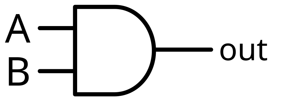 AND gate logic symbol diagram (Image: Public domain, via Wikimedia Commons)
The symbol consists of a flat‑faced rectangle with two input lines (A, B) entering from the left and one output line (Y) exiting to the right.
Truth Table
| A | B | Y = A · B |
|---|---|---|
| 0 | 0 | 0 |
| 0 | 1 | 0 |
| 1 | 0 | 0 |
| 1 | 1 | 1 |
Only when both inputs are true does the output become true.
Venn Diagram
The shaded overlap of sets A and B corresponds to the logical product A · B.
NAND Gate
The NAND gate is the complement of the AND gate; it produces a false output only when all its inputs are true.
Logic Symbol
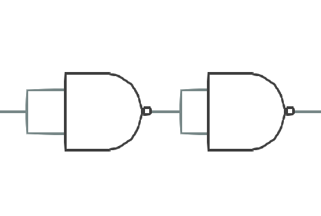 NAND gate logic symbol diagram (Image: A2569875, Public domain, via Wikimedia Commons)
The symbol is identical to the AND gate but with a small circle (the NOT bubble) at the output terminal, indicating inversion.
Truth Table
| A | B | Y = ¬(A · B) |
|---|---|---|
| 0 | 0 | 1 |
| 0 | 1 | 1 |
| 1 | 0 | 1 |
| 1 | 1 | 0 |
Thus the output is 0 only for the input combination 1, 1; otherwise it is 1.
Venn Diagram
The diagram shows that the NAND operation is true for every part of the universal set U except the intersection of A and B.
Comparison of AND and NAND
| Feature | AND Gate | NAND Gate |
|---|---|---|
| Logical function | Conjunction (A · B) | Negated conjunction ¬(A · B) |
| Symbol | Flat‑faced rectangle | Same rectangle with a NOT bubble |
| Output when A=1, B=1 | 1 | 0 |
| Output when any input = 0 | 0 | 1 |
| Universality | Not universal alone | Universal; any Boolean function can be built using only NAND gates |
| Implementation cost | Slightly lower (no inversion) | Slightly higher (requires extra transistor for inversion) |
Practical Note
In digital electronics, the NAND gate is preferred for building complex circuits because it is functionally complete: any Boolean expression can be realized using only NAND gates. This property reduces inventory, simplifies layout, and often leads to lower power consumption.
Discussion
Loading…