PhysicsUnit 2511 min read
Solids and Semiconductors – Crystal Structures, Band Theory, Doping and Devices
Unit 25 of Physics explores the atomic arrangement in solids (crystal structures), how electrons behave in energy bands, how semiconductors are doped to make diodes and transistors, and their real-world applications in electronics.
TAKEAWAYS:
- Solids are classified by their atomic arrangement (crystalline vs. amorphous) and bonding (metallic, ionic, covalent).
- In crystals, atoms repeat in unit cells (cubic, hexagonal, etc.), affecting properties like conductivity and strength.
- Band theory explains why metals conduct, insulators block, and semiconductors (like Si, Ge) have a small band gap that can be controlled.
- Doping (adding impurities) turns semiconductors into n-type (extra electrons) or p-type (holes), enabling pn-junction diodes and transistors.
- Semiconductor devices like LEDs, solar cells, and ICs rely on doped semiconductors and pn-junctions.
- Superconductors (below a critical temperature) have zero resistance and are used in MRI machines and maglev trains.
---

### **1. Classification of Solids**
Solids can be divided into two main types based on their **atomic arrangement**:
- **Crystalline solids**: Atoms/molecules are arranged in a **regular, repeating 3D pattern** (e.g., diamond, table salt, silicon).
- **Amorphous solids**: No long-range order (e.g., glass, rubber, plastic).

#### **Why does arrangement matter?**
The **type of bonding** (metallic, ionic, covalent) and **atomic spacing** determine properties like:
- **Conductivity** (metals conduct; ceramics do not).
- **Hardness** (diamond is hard because of strong covalent bonds).
- **Melting point** (ionic solids like NaCl melt at high temperatures).


---

### **2. Crystal Structures**
Crystals are built from **unit cells** (the smallest repeating block). Three common types:

#### **A. Cubic Unit Cells**
1. **Simple Cubic (SC)**
   - Atoms at **corners only** (1 atom per unit cell).
   - Example: Polonium (Po).
   - **Coordination number (CN)**: 6 (each atom touches 6 neighbors).
   - **Packing efficiency**: 52% (lots of empty space!).

2. **Body-Centered Cubic (BCC)**
   - Atoms at **corners + 1 in the center**.
   - Example: Iron (Fe), Tungsten (W).
   - CN: 8.
   - Packing efficiency: 68%.

3. **Face-Centered Cubic (FCC)**
   - Atoms at **corners + centers of all faces**.
   - Example: Copper (Cu), Gold (Au), Aluminum (Al).
   - CN: 12.
   - Packing efficiency: **74%** (most efficient packing!).


#### **B. Hexagonal Close-Packed (HCP)**
- Atoms in **two layers**: first layer (A), second layer (B) fits into the gaps of the first.
- Example: Magnesium (Mg), Zinc (Zn).
- CN: 12 (same as FCC).
- Packing efficiency: **74%** (same as FCC).

```figure
{"type":"layers","layers":["Layer A","Layer B"],"top":"Hexagonal packing","bottom":"Atoms in gaps","highlight":["Layer B"],"caption":"HCP structure: Layer B atoms sit in the depressions of Layer A"}
C. Diamond and Zinc Blende (ZnS) Structures
- Diamond (C): Each carbon atom is covalently bonded to 4 neighbors in a tetrahedral arrangement.
- Zinc Blende (ZnS): Zn²⁺ and S²⁻ ions alternate in an FCC lattice.
- Used in semiconductors (Si, Ge) and jewelry (diamond).
3. Bonding in Solids
| Type of Bonding | Examples | Properties | Conductivity |
|---|---|---|---|
| Metallic | Cu, Fe, Al | Free electrons (sea of electrons), malleable, shiny. | High (electrons move freely) |
| Ionic | NaCl, CaF₂ | Strong electrostatic forces, brittle, high melting point. | Low (no free electrons) |
| Covalent | Diamond, Si, C (graphite) | Very strong bonds, hard, high melting point. | Low (except graphite) |
| Van der Waals | Ice, Dry Ice (CO₂) | Weak forces, soft, low melting point. | Low |
4. Band Theory of Solids
Electrons in solids occupy energy bands (allowed energy levels). The band gap (Eg) is the energy difference between:
- Valence band (VB): Electrons are bound to atoms.
- Conduction band (CB): Electrons can move freely (conduct electricity).
Types of Solids Based on Band Gap
| Type | Band Gap (Eg) | Conductivity | Examples |
|---|---|---|---|
| Metals | 0 eV | High (overlap of VB & CB) | Cu, Al, Fe |
| Semiconductors | 1–4 eV | Medium (small Eg) | Si (1.1 eV), Ge (0.7 eV) |
| Insulators | > 4 eV | Very low (large Eg) | Diamond, Glass |
How does temperature affect conductivity?
- In metals: Conductivity decreases with temperature (electrons collide more).
- In semiconductors: Conductivity increases with temperature (more electrons jump to CB).
5. Semiconductors and Doping
Pure semiconductors (Si, Ge) have low conductivity because few electrons jump to the CB at room temperature. Doping adds impurities to increase conductivity.
A. Types of Doping
n-type (Negative) Doping
- Add Group 15 elements (P, As, Sb) which have 5 valence electrons.
- Extra electron becomes a free electron in the CB.
- Example: Si doped with P → n-type Si.
p-type (Positive) Doping
- Add Group 13 elements (B, Al, Ga) which have 3 valence electrons.
- Creates a hole (missing electron) in the VB.
- Example: Si doped with B → p-type Si.
B. pn-Junction Diodes
When p-type and n-type semiconductors are joined:
- Depletion region: No free charges (electrons and holes recombine).
- Barrier potential (0.7 V for Si): Prevents current flow in one direction.
flowchart TD
    A["p-type (holes)"] -->|"Holes diffuse to n-side"| B["Depletion region"]
    C["n-type (electrons)"] -->|"Electrons diffuse to p-side"| B
    B --> D["Barrier potential (0.7V)"]
    D --> E["Blocks current in reverse bias"]
    D --> F["Allows current in forward bias"]
C. Applications of Semiconductors
| Device | Working Principle | Applications |
|---|---|---|
| Diode | Allows current in one direction only. | Rectifiers, LEDs, solar cells. |
| Transistor | Acts as a switch or amplifier. | Radios, computers, smartphones. |
| LED | Electrons recombine with holes → light. | Displays, traffic lights. |
| Solar Cell | Light energy → electricity (photovoltaic effect). | Solar panels. |
| IC (Integrated Circuit) | Thousands of transistors on a chip. | CPUs, memory chips. |
6. Superconductors
- Definition: Materials with zero electrical resistance below a critical temperature (Tc).
- Meissner Effect: Expels magnetic fields (levitates magnets!).
- Examples:
- Conventional: Nb-Ti (Tc = 10 K), Hg (Tc = 138 K at high pressure).
- High-Tc: YBCO (Tc = 92 K), discovered in 1986.
Applications of Superconductors
- MRI machines (strong magnetic fields).
- Maglev trains (frictionless levitation).
- Power grids (zero energy loss).
7. Solved Examples
Example 1: Calculating Packing Efficiency
Problem: Calculate the packing efficiency of a simple cubic (SC) unit cell if the atomic radius is r. Solution:
- Volume of 1 atom = .
- Volume of unit cell = (since atoms touch along the edge).
- Number of atoms per unit cell in SC = 1 (only corners, each shared by 8 cells).
- Packing efficiency = = .
Example 2: Band Gap Calculation
Problem: Silicon has a band gap of 1.1 eV. At what temperature will thermal energy () equal the band gap? Solution:
- .
- Interpretation: At room temperature (300 K), , much smaller than 1.1 eV → few electrons jump to CB.
8. NEB Board-Style Questions
Short Answer Questions
Define "unit cell" and name two types of cubic unit cells.
- Answer: Smallest repeating unit in a crystal. Types: Simple Cubic (SC), Body-Centered Cubic (BCC), Face-Centered Cubic (FCC).
Why is diamond harder than graphite?
- Answer: Diamond has 3D covalent bonds; graphite has layers held by weak van der Waals forces.
What is doping? Name one n-type and one p-type dopant for silicon.
- Answer: Adding impurities to change conductivity. n-type: Phosphorus (P); p-type: Boron (B).
Explain the working of a pn-junction diode.
- Answer: In forward bias, the barrier is reduced → current flows. In reverse bias, the barrier increases → no current (except small leakage).
Long Answer Questions
With a neat diagram, explain the FCC unit cell and calculate its packing efficiency.
- Answer:
- Diagram: Show atoms at corners and face centers.
- Calculation:
- Atoms per unit cell = 8 corners × 1/8 + 6 faces × 1/2 = 4 atoms.
- Volume of unit cell = (edge length = ).
- Packing efficiency = .
- Answer:
Describe the band theory of solids. How does temperature affect the conductivity of a semiconductor?
- Answer:
- Band theory: Electrons occupy VB and CB, separated by Eg.
- Temperature effect: Higher T → more electrons jump to CB → conductivity increases.
- Answer:
Exam Tip
Diagrams are key! Always draw:
- Unit cells (SC, BCC, FCC).
- Band diagrams for metals, semiconductors, insulators.
- pn-junction with depletion region.
Memorize these values:
- Band gap of Si = 1.1 eV, Ge = 0.7 eV.
- Packing efficiencies: SC (52%), BCC (68%), FCC/HCP (74%).
Common mistakes to avoid:
- Confusing n-type (extra electrons) and p-type (holes).
- Forgetting that doping increases conductivity in semiconductors.
- Misdrawing the depletion region in a pn-junction.
Application-based questions are common. Relate concepts to real devices:
- Diodes → Rectifiers in power supplies.
- Transistors → Amplifiers in radios.
- Superconductors → MRI machines.
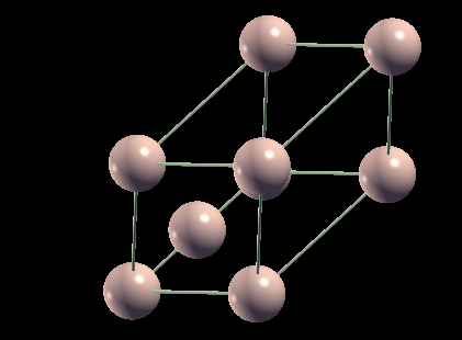 A close-up view of silicon’s diamond-like atomic arrangement. (Image: MmRoma, CC0, via Wikimedia Commons)
Based on the NEB +2 Science syllabus for Physics (Phy), unit 25.
Discussion
Loading…