Electronic Devices and CircuitsUnit 28 min read
PN Junction Diode: IV Curve, Biasing, Applications & Models
Unit 2 of Electronic Devices and Circuits covers the PN junction diode’s construction, IV characteristics, biasing (forward/reverse), equivalent circuit models (ideal/real), and real-world applications in rectifiers, voltage regulation, and signal processing—with visuals of gate symbols, IV curves, and actual diode chi
Key Concepts and Theory
1. PN Junction Formation and Depletion Region
A PN junction is formed when a p-type (hole-rich) and n-type (electron-rich) semiconductor are brought into contact. At the junction, electrons from the n-side diffuse to the p-side and recombine with holes, creating a depletion region (a region devoid of free charge carriers). This region establishes an electric field (barrier potential, ~0.7V for Si, ~0.3V for Ge) that opposes further diffusion.
   p-type (holes)       n-type (electrons)
   ----------------------------
   + + + + + +           - - - - - -
   (acceptor ions)       (donor ions)
   ----------------------------
   Depletion Region (E-field)
   ----------------------------
Key Points:
- The depletion region width increases with reverse bias and decreases with forward bias.
- The built-in potential () is the voltage required to reduce the depletion region to zero under forward bias.
2. IV Characteristics of a PN Junction Diode
The current-voltage (I-V) relationship of a diode is given by the Shockley diode equation: where:
- = diode current,
- = reverse saturation current (~pA to nA),
- = applied voltage,
- = emission coefficient (~1–2 for Si),
- = thermal voltage (~26 mV at 300 K).
Visual: IV Curve
   I (A)
   |
   |       /-------
   |      /
   |     /
   |____/__________ V (V)
      -Vr   0   Vf
- Forward Bias (V > 0): Current increases exponentially after the knee voltage (~0.6–0.7V for Si).
- Reverse Bias (V < 0): Current is nearly constant () until breakdown (avalanche or Zener).
Worked Example: A silicon diode has A and . Calculate at V.
3. Biasing of PN Junction Diode
Biasing determines the operating point of a diode. There are two primary modes:
| Bias Type | Voltage Applied | Depletion Region | Current Flow | Applications |
|---|---|---|---|---|
| Forward Bias | Narrows | High () | Rectifiers, Logic Gates, LEDs | |
| Reverse Bias | Widens | Low () | Voltage Regulators, Zener Diodes |
Real-World Example:
- eSewa App (Nepal): Uses diodes in rectifier circuits to convert AC from the grid to DC for charging mobile wallets during power outages.
- Khalti Payments: Diodes in voltage regulators ensure stable power supply to servers handling transactions.
4. Equivalent Circuit Models
Diodes are modeled in two ways for circuit analysis:
A. Ideal Diode Model
- Assumes:
- Zero forward voltage drop ().
- Infinite resistance in reverse bias.
- Limitations: Ignores real-world behavior (e.g., knee voltage, leakage).
B. Practical Diode Model
- Forward Bias: (e.g., 0.7V for Si).
- Reverse Bias: (leakage current).
- Breakdown: (Zener voltage).
Visual: Diode Models
5. Diode Applications
A. Rectifiers (AC to DC Conversion)
Half-Wave Rectifier:
AC Input | [Diode] -->|Output| [Load] | Ground- Output: Pulsating DC (only positive half-cycles).
- Efficiency: ~40.6%.
Full-Wave Rectifier (Center-Tapped or Bridge):
- Output: Both half-cycles used.
- Efficiency: ~81.2%.
Worked Example (Nepal Context): NTC (Nepal Electricity Authority) uses bridge rectifiers in substations to convert 230V AC from transmission lines to DC for electrolysis plants (e.g., chlorine production). If the input is 230V RMS, calculate the peak output voltage (ignoring diode drops).
B. Clipping and Clamping Circuits
- Clipper: Removes a portion of the input signal.
- Clamper: Shifts the DC level of the input signal.
Visual: Clipping Circuit
   Vin
    |
   [Diode] -->|Vout| [Load]
    |       |
   ---      ---
   GND     Vref
C. Voltage Regulation (Zener Diode)
- Zener Diode: Operates in reverse breakdown to maintain a constant voltage.
- Example: In Ncell’s base stations, Zener diodes regulate voltage for sensitive RF amplifiers.
Worked Example: A Zener diode with V and mA is used to regulate voltage. If the load current is 10 mA, calculate the required series resistor for an input of 12 V.
6. Temperature Effects
- Forward Voltage Drop (): Decreases by ~2 mV/°C.
- Reverse Leakage Current (): Doubles for every 10°C rise.
- Impact: Circuits must include temperature compensation (e.g., using thermistors).
In the Real World
Pathao (Ride-Hailing App):
- Uses bridge rectifiers in its GPS modules to power the device from AC adapters during charging.
- Why? Ensures stable DC power for accurate location tracking.
Daraz (E-Commerce):
- Clamping circuits protect order-processing servers from voltage spikes during lightning strikes.
- Example: A TVS (Transient Voltage Suppressor) diode clamps spikes to safe levels (~5.1V).
Nepal Rastra Bank (NRB) ATMs:
- Zener diodes regulate power supplies for secure transaction processing.
- Scenario: If input voltage spikes to 15V, a 5V Zener ensures the ATM’s logic board sees a stable 5V.
Exam Tip
Memorize Key Values:
- Silicon diode V, Germanium V.
- Zener breakdown voltages (e.g., 3.3V, 5.1V, 12V) are common in exams.
Graphical Analysis:
- Always sketch the IV curve and mark:
- Knee voltage,
- Reverse saturation current,
- Breakdown region.
- For rectifiers, plot input/output waveforms (half-wave vs. full-wave).
- Always sketch the IV curve and mark:
Circuit Analysis:
- Assume ideal diodes unless specified otherwise.
- For practical diodes, account for drops in forward bias.
- In Zener applications, calculate series resistance using .
Common Pitfalls:
- Forgetting to include in reverse bias calculations.
- Misidentifying forward vs. reverse bias in circuit diagrams.
- Ignoring temperature effects in real-world scenarios (e.g., "Why does the diode fail in summer?").
Numerical Problems:
- Rectifiers: Calculate , , and ripple factor.
- Clippers/Clampers: Determine output voltage levels using diode polarity.
- Zener Regulators: Solve for or in the Zener.
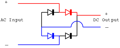 Four-diode arrangement for full-wave rectification. (Image: MichaelOReilly at English Wikipedia, Public domain, via Wikimedia Commons)
Based on the PU BE Computer (PU) syllabus for Electronic Devices and Circuits (ELX120), unit 2.
Discussion
Loading…