Electronic Devices and CircuitsUnit 419 min read
Special Diodes: Zener, Varactor, LED, Photodiode, Schottky & Tunnel
Unit 4 of Electronic Devices and Circuits covers six specialized diodes—Zener, varactor, LED, photodiode, Schottky, and tunnel—explaining their construction, working principles, unique characteristics, and practical applications in voltage regulation, sensing, and optoelectronics, with real-world examples from Nepalese
Key Concepts and Devices
1. Zener Diode
Definition and Construction
A Zener diode is a heavily doped PN-junction diode designed to operate in the reverse-bias breakdown region. Unlike regular diodes, it is intentionally operated in this region to exploit the Zener breakdown (for voltages < 5V) or **avalanche breakdown** (for voltages > 5V). The doping levels are extremely high (10^19 to 10^20 atoms/cm³), creating a thin depletion region (~1 µm).
Working Principle
- Reverse Bias: When a reverse voltage exceeds the Zener voltage (), electrons tunnel through the depletion region, allowing current to flow without damage.
- Voltage Regulation: The Zener diode maintains a nearly constant output voltage despite input voltage variations, making it ideal for voltage regulators.
Key Parameters
| Parameter | Symbol | Typical Value (Example: 5.1V Zener) | Description |
|---|---|---|---|
| Zener Voltage | 5.1V | Voltage at which breakdown occurs. | |
| Zener Current | 20mA | Current through the diode in breakdown. | |
| Test Current | 200mA | Current used to measure (usually 10× ). | |
| Dynamic Resistance | 10Ω | (lower = better regulation). | |
| Power Dissipation | 500mW | Maximum power the diode can dissipate without overheating. |
Circuit Symbol and Real Picture
Applications
- Voltage Regulators: Used in power supplies (e.g., laptop chargers, phone chargers) to provide stable DC voltages.
- Voltage References: In precision circuits (e.g., sensor signal conditioning).
- Overvoltage Protection: Protects sensitive circuits (e.g., Ncell SIM cards, eSewa payment gateways) from voltage spikes.
- Clipping Circuits: Limits voltage in amplifiers (e.g., audio signal processing).
Worked Example: Zener Diode as a Voltage Regulator
Problem: Design a simple voltage regulator to provide from an input voltage ranging from 10V to 15V. The load current is 10mA, and the Zener diode has , , and .
Solution:
- Choose a Zener Diode: Select a 5.1V Zener (e.g., 1N4733A).
- Calculate Minimum : To ensure regulation, must be at least 5mA even when is maximum.
- .
- Select Resistor :
- At , : .
- At , check power dissipation: , (safe).
- Final Circuit:
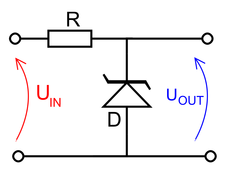 A simple Zener regulator with input voltage, resistor, and load. (Image: CC BY-SA 3.0, via Wikimedia Commons)
#### Advantages and Disadvantages
| Advantages                          | Disadvantages                          |
|--------------------------------------|----------------------------------------|
| Simple and inexpensive.              | Limited to specific voltage levels.    |
| Fast response time.                  | Power dissipation limits output current. |
| High reliability.                    | Requires heat sinking for high power.  |
| Used in both low and high voltage apps. | Sensitive to temperature variations.   |

---

### 2. **Varactor Diode (Varicap Diode)**

```figure
{"type":"graph","fns":[{"expr":"1/(1 + 1000*(x-5)^2)","label":"C_j (pF) vs. Reverse Voltage (V)"}],"x":[0,10],"y":[0,100],"caption":"Varactor diode capacitance vs. reverse voltage (typical tuning range)."}
Definition and Construction
A varactor diode is a reverse-biased PN-junction diode designed to exploit the voltage-dependent capacitance of its depletion region. It is lightly doped to create a wide depletion region, whose capacitance changes with applied reverse voltage.
Working Principle
- Capacitance Variation: The depletion region width increases with reverse voltage, reducing capacitance (, where is depletion width).
- Non-linear Capacitance: Used in tuning circuits where precise capacitance control is needed.
Key Parameters
| Parameter | Symbol | Typical Range | Description |
|---|---|---|---|
| Capacitance Ratio | 2:1 to 10:1 | Ratio of capacitance at 0V to maximum reverse voltage. | |
| Maximum Reverse Voltage | 5V to 100V | Maximum voltage before breakdown. | |
| Quality Factor | 100 to 1000 | Measures efficiency (higher = better for RF applications). |
Circuit Symbol and Real Picture
Applications
- Tuning Circuits: Used in radio receivers (e.g., NTC FM radios) to adjust resonance frequency.
- Frequency Modulation (FM): In FM transmitters (e.g., community radio stations) to vary oscillator frequency.
- Phase-Locked Loops (PLL): Used in clock generation circuits (e.g., microcontroller oscillators).
- Voltage-Controlled Oscillators (VCO): In synthesizers and wireless communication (e.g., Ncell 4G modems).
Worked Example: Varactor Diode in an FM Tuner
Problem: A varactor diode in an FM radio tuner has at 0V and at 10V. Calculate the tuning range if the inductor .
Solution:
- Resonance Frequency Formula: .
- Calculate Frequencies:
- At : .
- At : .
- Tuning Range: Covers 88MHz to 108MHz (typical FM band) if adjusted properly.
3. Light Emitting Diode (LED)
Definition and Construction
An LED is a PN-junction diode that emits light when forward-biased. It is made from semiconductor materials with a direct bandgap (e.g., GaAs, GaP, InP, AlGaInP). The recombination of electrons and holes releases energy as photons.
Working Principle
- Forward Bias: Electrons from the N-side recombine with holes on the P-side, releasing energy as visible light.
- Wavelength: Determined by the bandgap energy ():
- Red LED: ~650nm (GaAsP)
- Green LED: ~520nm (GaP)
- Blue LED: ~470nm (GaN)
- White LED: Combines blue LED + phosphor coating.
Key Parameters
| Parameter | Symbol | Typical Value (Red LED) | Description |
|---|---|---|---|
| Forward Voltage | 1.8V to 2.2V | Voltage drop across LED when lit. | |
| Forward Current | 10mA to 30mA | Typical operating current. | |
| Peak Wavelength | 650nm | Wavelength of emitted light. | |
| Viewing Angle | 20° to 160° | Angular range over which light is emitted. | |
| Luminous Intensity | 1000mcd | Brightness of the LED. |
Circuit Symbol and Real Picture

Applications
- Indicators: Used in power supplies, mobile phones, and traffic lights.
- Displays: 7-segment displays (e.g., digital clocks, microwave ovens).
- Lighting: Street lights, TV backlights, and home lighting (e.g., LED bulbs in Nepalese homes).
- Optical Communication: Fiber optics (e.g., internet backbone cables).
- Automotive: Brake lights, dashboard indicators (e.g., Toyota Prius LEDs).
Worked Example: LED Circuit Design
Problem: Design a circuit to light a red LED (, ) from a 5V supply.
Solution:
- Current Limiting Resistor: Use .
- Power Dissipation: (safe for standard resistors).
- Final Circuit:
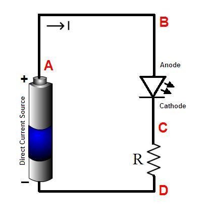 A simple LED circuit with a current-limiting resistor. (Image: CC0, via Wikimedia Commons)
#### Advantages and Disadvantages
| Advantages | Disadvantages |
|--------------------------------------|----------------------------------------|
| Low power consumption. | Lower brightness than incandescent bulbs (older LEDs). |
| Long lifespan (~100,000 hours). | Sensitive to static electricity. |
| Fast switching (~ns). | Narrow viewing angle in some types. |
| Eco-friendly (no mercury). | Higher initial cost than incandescent. |
| Compact size. | Requires precise current control. |
---
### 4. **Photodiode**
#### Definition and Construction
A **photodiode** is a **reverse-biased PN-junction diode** designed to convert **light into electrical current**. It operates in **photoconductive mode** (zero bias) or **photovoltage mode** (reverse bias). Materials include **Si, Ge, InGaAs** (for different wavelength ranges).
#### Working Principle
- **Photoconductive Mode**: Light generates electron-hole pairs, increasing reverse current ().
- **Photovoltage Mode**: Light creates a small voltage across the diode (used in solar cells).
- **Reverse Bias**: Increases depletion region width, improving sensitivity.
#### Key Parameters
| Parameter | Symbol | Typical Value (Si Photodiode) | Description |
|-------------------------|--------|--------------------------------|-----------------------------------------------------------------------------|
| Dark Current | | 1nA to 1µA | Current with no light (leakage). |
| Responsivity | | 0.5A/W | Current generated per unit optical power. |
| Rise Time | | 1ns to 100ns | Speed of response to light changes. |
| Wavelength Range | | 200nm to 1100nm | Spectral range of sensitivity. |
#### Circuit Symbol and Real Picture
#### Applications
- **Light Sensors**: **Automatic street lights** (e.g., **NTC smart street lights**).
- **Optical Communication**: **Fiber optic receivers** (e.g., **internet routers**, **Nepal Telecom fiber networks**).
- **Barcode Scanners**: Used in **retail POS systems** (e.g., **Daraz barcode readers**).
- **Medical Devices**: **Pulse oximeters** (measure oxygen levels in blood).
- **Consumer Electronics**: **Camera modules** (e.g., **smartphone cameras**).
#### Worked Example: Photodiode in a Light Sensor
**Problem**: A photodiode has a responsivity of and a dark current of . Calculate the output current when illuminated by a 1mW light source.
**Solution**:
1. **Photo Current**: .
2. **Total Current**: (dark current negligible).
---
### 5. **Schottky Diode**
#### Definition and Construction
A **Schottky diode** is a **metal-semiconductor junction diode** (not PN-junction) formed by a **metal (e.g., platinum, aluminum) and an N-type semiconductor**. It has a **very thin depletion region**, enabling **fast switching**.
#### Working Principle
- **Majority Carrier Operation**: Only electrons (in N-type) contribute to conduction, reducing capacitance and improving speed.
- **Low Forward Voltage Drop**: Typically **0.2V to 0.3V** (vs. 0.6V–0.7V for silicon PN diodes).
- **No Minority Carrier Storage**: Enables **high-frequency operation**.
#### Key Parameters
| Parameter | Symbol | Typical Value (Silicon Schottky) | Description |
|-------------------------|--------|-----------------------------------|-----------------------------------------------------------------------------|
| Forward Voltage | | 0.2V to 0.3V | Lower than PN diodes. |
| Reverse Recovery Time | | <1ns | Extremely fast (no minority carriers). |
| Maximum Current | | 1A to 100A | Depends on package size. |
| Breakdown Voltage | | 20V to 200V | Lower than PN diodes for same technology. |
#### Circuit Symbol and Real Picture
#### Applications
- **High-Speed Switching**: **Clock circuits**, **RF amplifiers** (e.g., **5G base stations**).
- **Power Supplies**: **Flyback converters**, **switching regulators** (e.g., **laptop chargers**).
- **Reverse Polarity Protection**: **USB ports**, **battery chargers**.
- **Logic Circuits**: **TTL and CMOS interfaces** (e.g., **microcontroller I/O pins**).
#### Worked Example: Schottky Diode in a Flyback Converter
**Problem**: A flyback converter uses a Schottky diode with and . Calculate the power saved compared to a silicon PN diode () at 1A.
**Solution**:
1. **Power Loss in Schottky Diode**: .
2. **Power Loss in PN Diode**: .
3. **Savings**: (40% reduction).
---
### 6. **Tunnel Diode**
#### Definition and Construction
A **tunnel diode** is a **heavily doped PN-junction diode** that exhibits **negative resistance** due to **quantum tunneling**. It operates in the **forward bias region** where current decreases with increasing voltage.
#### Working Principle
- **Tunneling Effect**: Electrons tunnel through the thin depletion region without thermal energy.
- **Negative Resistance Region**: Between **peak current ()** and **valley current ()**, the diode behaves as a negative resistor ().
#### Key Parameters
| Parameter | Symbol | Typical Value | Description |
|-------------------------|--------|---------------|-----------------------------------------------------------------------------|
| Peak Current | | 1mA to 100mA | Maximum current in the negative resistance region. |
| Valley Current | | 0.1mA to 10mA | Minimum current in the negative resistance region. |
| Peak Voltage | | 50mV to 100mV | Voltage at . |
| Valley Voltage | | 200mV to 500mV| Voltage at . |
| Switching Speed | | <1ns | Extremely fast due to majority carrier operation. |
#### Circuit Symbol and Real Picture
#### Applications
- **Oscillators**: **Microwave oscillators**, **RF amplifiers** (e.g., **radar systems**).
- **High-Speed Switching**: **Logic circuits**, **memory elements**.
- **Amplifiers**: **Low-noise amplifiers** (e.g., **satellite communication**).
- **Relaxation Oscillators**: Used in **timing circuits**.
#### Worked Example: Tunnel Diode Oscillator
**Problem**: A tunnel diode has , , and . Design a simple oscillator using an inductor .
**Solution**:
1. **Negative Resistance**: The tunnel diode provides negative resistance in the to region.
2. **Resonant Circuit**: Combine with an inductor to form a **relaxation oscillator**.
3. **Frequency**: Depends on and the diode’s characteristics (typically **GHz range** for microwave apps).
---
## In the Real World
1. **eSewa and Khalti Payments**:
- **Zener Diodes**: Used in **voltage regulators** within payment terminals to ensure stable 5V for microcontrollers and sensors.
- **Schottky Diodes**: Found in **fast switching circuits** for secure transaction processing.
2. **Pathao and Daraz Logistics**:
- **Photodiodes**: Used in **barcode scanners** for inventory management and package tracking.
- **LEDs**: Indicate order status (e.g., "order confirmed," "delivery in progress").
3. **Nepal Telecom (NTC) and Ncell Networks**:
- **Varactor Diodes**: Tuning circuits in **4G/5G base stations** to adjust frequencies dynamically.
- **Schottky Diodes**: High-speed switching in **power amplifiers** for signal transmission.
4. **Nepal Stock Exchange (NEPSE) Trading Terminals**:
- **LEDs**: Display stock prices and trade status in real-time.
- **Zener Diodes**: Protect sensitive trading software from power surges.
5. **Kathmandu Traffic Management**:
- **Photodiodes**: Used in **traffic light sensors** to detect vehicles and adjust signal timings dynamically.
---
## Exam Tip
1. **Memorize Key Values**:
- Zener diode voltages (e.g., 3.3V, 5.1V, 6.8V) and their typical applications.
- LED forward voltages (red: 1.8V, blue: 3.2V, white: 3.0V).
- Schottky diode forward voltage (~0.3V) vs. PN diode (~0.7V).
2. **Circuit Analysis**:
- Always draw the **complete circuit** (including load) when solving problems.
- For Zener regulators, calculate **minimum ** to ensure regulation.
- For LEDs, **never forget the current-limiting resistor**.
3. **Graphs and Characteristics**:
- Sketch the **I-V curve** for Zener, tunnel, and Schottky diodes, highlighting unique regions (e.g., negative resistance in tunnel diodes).
- Plot **capacitance vs. voltage** for varactor diodes.
4. **Applications**:
- Link diodes to **real-world systems** (e.g., "Zener diode in a laptop charger" or "photodiode in a barcode scanner").
- Explain **why** a specific diode is chosen (e.g., Schottky for speed, LED for visibility).
5. **Common Pitfalls**:
- **Polarity**: Always check diode polarity in circuits (anode to cathode for forward bias).
- **Power Dissipation**: Ensure Zener diodes are not overheated (calculate ).
- **Wavelength**: Match LED/photodiode materials to the application (e.g., InGaAs for IR).
6. **Practical Questions**:
- Expect **design problems** (e.g., "Design a circuit to light an LED from a 9V battery").
- Be ready for **comparison questions** (e.g., "Compare Zener and Schottky diodes for a voltage regulator").
---
Based on the PU BE Computer (PU) syllabus for Electronic Devices and Circuits (ELX120), unit 4.
Discussion
Loading…