PhysicsUnit 89 min read
Digital Logic & IC Fabrication: Gates, Circuits & Semiconductor Processes
Unit 8 of Physics covers digital logic families (RTL/TTL), logic gate design, truth tables, Boolean algebra implementation, and the step-by-step fabrication of integrated circuits (ICs) using silicon processing techniques.
TAKEAWAYS:
- Logic gates (AND, OR, NOT, NAND, NOR) are the building blocks of digital circuits, implemented using transistors in ICs.
- RTL (Resistor-Transistor Logic) and TTL (Transistor-Transistor Logic) are two key digital logic families with distinct speed/power trade-offs.
- Boolean algebra converts logical expressions into gate-level circuits via truth tables, Karnaugh maps, and De Morgan’s laws.
- IC fabrication follows a photolithography-based process: oxidation → doping → etching → metallization, creating transistors and interconnects on silicon wafers.
- Memory and clock circuits rely on feedback loops (flip-flops) and oscillators built from gates, enabling sequential logic.
- Real-world applications span from mobile apps (e.g., Pathao’s order routing) to hardware (e.g., Ncell’s baseband processors).
1. Digital Logic Gates: Theory and Implementation
Digital circuits process binary signals (0/1) using logic gates, which perform basic operations. Gates are classified by their function:
Basic Gates and Symbols
classDiagram
    class AND_Gate {
        +Output = A AND B
        +Symbol: AND
    }
    class OR_Gate {
        +Output = A OR B
        +Symbol: OR
    }
    class NOT_Gate {
        +Output = NOT A
        +Symbol: NOT
    }
    class NAND_Gate {
        +Output = NOT (A AND B)
        +Symbol: AND + NOT
    }
    class NOR_Gate {
        +Output = NOT (A OR B)
        +Symbol: OR + NOT
    }
    AND_Gate --> "Universal" NAND_Gate : "Can replace"
    OR_Gate --> "Universal" NOR_Gate : "Can replace"
Key Gates:
- AND: Outputs
1only if all inputs are1. - OR: Outputs
1if any input is1. - NOT (Inverter): Inverts the input (
0→1,1→0). - NAND/NOR: Universal gates (can implement any logic function).
Truth Tables and Boolean Algebra
A truth table lists all possible input combinations and their corresponding outputs. For example, the XOR gate (exclusive OR) outputs 1 only when inputs differ:
| A | B | A XOR B |
|---|---|---|
| 0 | 0 | 0 |
| 0 | 1 | 1 |
| 1 | 0 | 1 |
| 1 | 1 | 0 |
Boolean Algebra Rules (Critical for Simplification):
- Commutative: ,
- Associative:
- Distributive:
- De Morgan’s Laws:
Worked Example: Simplify Using Boolean algebra: This simplifies to (since is absorbed by ).
2. Digital Logic Families: RTL vs. TTL
Digital circuits use different logic families, each with trade-offs in speed, power, and cost.
Comparison Table
| Feature | RTL (Resistor-Transistor Logic) | TTL (Transistor-Transistor Logic) |
|---|---|---|
| Speed | Slow (~10 MHz) | Fast (~30–100 MHz) |
| Power | Low (10–20 mW) | Medium (10–100 mW) |
| Fan-Out | Limited (1–2) | High (8–10) |
| Noise Immunity | Poor (0.3V) | Good (0.4V) |
| Implementation | Discrete transistors + resistors | Integrated transistors (ICs) |
| Example ICs | None (obsolete) | 7400 series (e.g., 74LS00 NAND gate) |
How TTL Works
TTL uses bipolar junction transistors (BJTs) in a totem-pole output stage for high drive strength:
- Input Stage: Resistor-transistor pair senses voltage levels.
- Phase-Splitter Stage: Inverts and amplifies the signal.
- Output Stage: Push-pull configuration (transistors act as source/sink for current).
Advantages of TTL:
- High speed (used in early computers like the Apple I).
- Easy to interface with other circuits.
- Disadvantage: Higher power consumption than CMOS (modern alternative).
3. Designing Circuits from Boolean Expressions
Step-by-Step Process
- Write the Boolean expression (e.g., ).
- Draw the circuit using gates:
- Parentheses → AND/OR grouping.
- Overbars → NOT gates.
- Verify with a truth table.
Example: Implement (XOR)
flowchart TD
    A["Input A"] --> NOTB["NOT B"]
    B["Input B"] --> NOTA["NOT A"]
    NOTB --> AND1["AND"]
    NOTA --> AND2["AND"]
    A --> AND1
    B --> AND2
    AND1 --> OR["OR"]
    AND2 --> OR
    OR --> Y["Output Y"]
Truth Table Verification:
| A | B | Y | ||||
|---|---|---|---|---|---|---|
| 0 | 0 | 1 | 1 | 0 | 0 | 0 |
| 0 | 1 | 0 | 1 | 0 | 1 | 1 |
| 1 | 0 | 1 | 0 | 1 | 0 | 1 |
| 1 | 1 | 0 | 0 | 0 | 0 | 0 |
4. Memory and Clock Circuits Using Gates
A. Flip-Flops (Memory)
A SR (Set-Reset) latch is the simplest memory element, built from NAND/NOR gates:
flowchart TD
    S["Set"] --> NAND1["NAND"]
    R["Reset"] --> NAND2["NAND"]
    NAND1 --> Q["Q (Output)"]
    NAND2 --> QB["Q' (Complement)"]
    Q --> NAND2
QB --> NAND1- State Retention: Outputs and reinforce each other.
- Applications: Registers, counters, RAM.
B. Astable Multivibrator (Clock)
A 555 timer IC (used in clocks) can be built from gates:
flowchart TD
    VCC["+5V"] --> NOT1["NOT Gate"]
    NOT1 --> CAP["Capacitor"]
    CAP --> NOT2["NOT Gate"]
    NOT2 --> OUT["Clock Output"]
OUT --> NOT1- Oscillation: Feedback creates a square-wave clock signal.
- Frequency: .
Real-World Tie-In:
- Pathao’s Order Routing: Uses flip-flops to track driver availability (memory) and timing circuits for delivery deadlines (clocks).
- Ncell’s Baseband Processor: Relies on TTL/CMOS gates for signal modulation/demodulation in 4G/5G chips.
5. Integrated Circuit (IC) Fabrication Process
ICs are fabricated using photolithography and doping on silicon wafers. Key steps:
Step-by-Step Process
flowchart TD
    A["Silicon Ingot"] --> B["Wafer Slicing"]
    B --> C["Oxidation: Grow SiO2"]
    C --> D["Photoresist Coating"]
    D --> E["Pattern Exposure (UV)"]
    E --> F["Etching: Remove Oxide"]
    F --> D["Repeat for Layers"]
    D --> G["Doping: Impurities"]
    G --> H["Metallization: Al/Cu"]
    H --> I["Testing & Packaging"]
Key Techniques:
- Oxidation: Grow layer (insulator).
- Photolithography: UV light + photoresist to define patterns.
- Etching: Remove exposed oxide (wet/dry etch).
- Doping: Add impurities (e.g., boron for p-type, phosphorus for n-type) to create transistors.
- Metallization: Deposit aluminum/copper for interconnects.
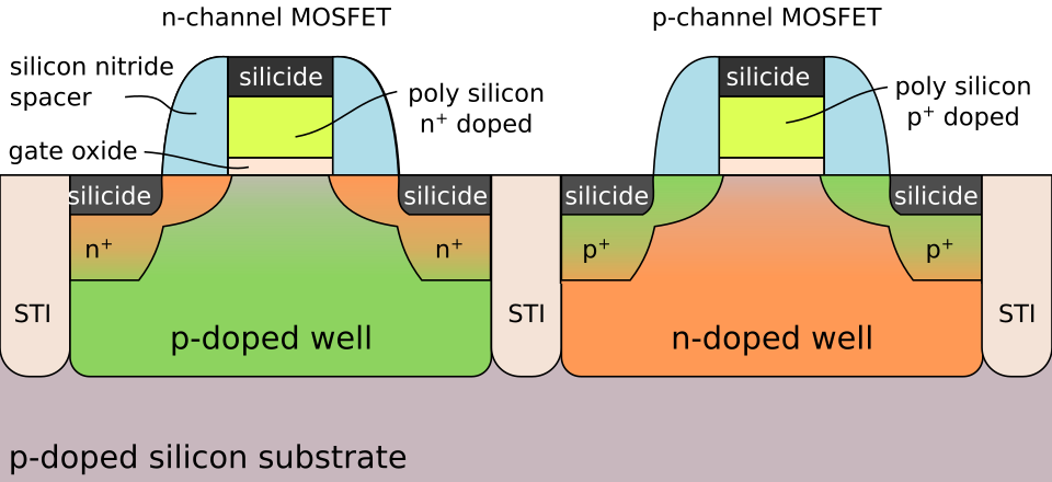 N-channel and P-channel MOSFETs in a silicon substrate. (Image: Cepheiden, CC BY-SA 3.0, via Wikimedia Commons)
Example: Fabricating a NAND Gate
- Start with a p-type silicon wafer.
- Grow and deposit photoresist.
- Expose to UV to define source/drain regions (n-type doping).
- Add polysilicon gate (conductive path).
- Deposit metal interconnects to link gates.
Real-World Tie-In:
- eSewa’s Payment Gateway: Relies on ICs fabricated via this process for secure encryption chips.
- NEPSE’s Trading Terminals: Use FPGAs (field-programmable gate arrays) built with similar techniques for real-time stock data processing.
6. Exam Tips
Truth Tables Are Non-Negotiable:
- Always verify your circuit with a truth table. Examiners check for completeness (all 16 combinations for 4 inputs).
- Example: For , list all 8 rows.
Gate Simplification:
- Use Karnaugh maps for 3–4 variables to simplify before drawing circuits.
- Memorize De Morgan’s laws for converting NAND/NOR to other gates.
IC Fabrication:
- Know the order of steps: Oxidation → Lithography → Doping → Metallization.
- Common Pitfalls:
- Mixing up n-type/p-type doping.
- Forgetting that photoresist is removed after etching.
RTL vs. TTL:
- RTL is obsolete; focus on TTL/CMOS for exams.
- Compare speed, power, and fan-out in tables.
Circuit Drawing:
- Use standard symbols (IEC/IEEE).
- Label inputs/outputs clearly (e.g., ).
Real-World Questions:
- Expect applications (e.g., "How is a clock circuit used in a smartphone?").
- Link Boolean logic to decision-making (e.g., traffic light controllers).
Final Note:
- Practice: Draw circuits for 5–10 Boolean expressions.
- Lab Work: Simulate gates in Logicly or Proteus to see waveforms.
- Formula Sheet: Memorize TTL voltage levels (VOH = 2.4V, VOL = 0.4V).
Based on the TU BSc CSIT syllabus for Physics (PHY118), unit 8.
Discussion
Loading…