PhysicsUnit 249 min read
Semiconductor Devices: Diodes, Transistors, ICs & Applications
Unit 24 of Physics explores how semiconductor devices like diodes, transistors, and integrated circuits work, their symbols, V-I characteristics, and real-world uses in electronics.
What Are Semiconductors?
Semiconductors are materials with electrical conductivity between conductors (like metals) and insulators (like rubber). Their conductivity can be controlled by adding impurities (doping) or by external factors like temperature and light.
Types of Semiconductors
There are two main types:
- Intrinsic Semiconductors: Pure semiconductors (e.g., pure silicon or germanium) with no impurities. Their conductivity is low.
- Extrinsic Semiconductors: Semiconductors doped with impurities to increase conductivity. These are further divided into:
- N-type: Doped with elements like phosphorus (5 valence electrons) that have extra free electrons.
- P-type: Doped with elements like boron (3 valence electrons) that create "holes" (positive charge carriers).
pie
    title Types of Semiconductors
    "Intrinsic" : 20
    "Extrinsic (N-type)" : 40
    "Extrinsic (P-type)" : 40
PN Junction and Diodes
A PN junction is formed when a P-type and an N-type semiconductor are joined together. This junction has unique electrical properties.
How a PN Junction Works
- When the junction is forward-biased (positive voltage to P-side, negative to N-side), the depletion region narrows, and current flows easily.
- When the junction is reverse-biased (negative voltage to P-side, positive to N-side), the depletion region widens, and very little current flows (except a small leakage current).
Diode: The Basic Semiconductor Device
A diode is a two-terminal device made from a PN junction. It allows current to flow in one direction only.
Symbol and V-I Characteristics
- Symbol:
flowchart TD
  A["P"] -->|"Anode"| B["Diode"]
  C["N"] -->|"Cathode"| B
- V-I Characteristics:
- In forward bias, the diode conducts current after a certain threshold voltage (≈0.7V for silicon).
- In reverse bias, the diode blocks current until the breakdown voltage is reached.
Example: Diode in a Circuit
Consider a diode connected in series with a resistor and a battery (forward-biased). The voltage across the diode is approximately 0.7V (for silicon). If the battery voltage is 5V and the resistor is 1kΩ, calculate the current through the circuit.
Solution:
- Voltage drop across resistor = 5V - 0.7V = 4.3V
- Current
Types of Diodes
Diodes come in various types, each with specific applications:
| Type of Diode | Symbol | Function |
|---|---|---|
| Rectifier Diode |  | Converts AC to DC. |
| Zener Diode |  | Used for voltage regulation in reverse bias. |
| LED (Light Emitting Diode) |  | Emits light when forward-biased. |
| Photodiode |  | Converts light into electrical current. |
| Varactor Diode |  | Used as a voltage-dependent capacitor in tuning circuits. |
Transistors: The Building Blocks of Modern Electronics
Transistors are three-terminal devices used to amplify or switch electronic signals. There are two main types:
- Bipolar Junction Transistor (BJT)
- Field Effect Transistor (FET)
Bipolar Junction Transistor (BJT)
A BJT has three regions: Emitter (E), Base (B), and Collector (C). It can be either NPN or PNP.
How BJT Works
- In active mode, a small current at the base controls a larger current between the collector and emitter.
- The current gain (β) is defined as: where is the collector current and is the base current.
Example: BJT Amplifier
Suppose a BJT has a current gain (β) of 100. If the base current is 20 µA, calculate the collector current .
Solution:
Field Effect Transistor (FET)
FETs are voltage-controlled devices with three terminals: Source (S), Gate (G), and Drain (D). They are classified into:
- JFET (Junction Field Effect Transistor)
- MOSFET (Metal-Oxide-Semiconductor Field Effect Transistor)
How MOSFET Works
- The gate voltage controls the conductivity between the source and drain.
- MOSFETs are widely used in digital circuits and integrated circuits (ICs) due to their low power consumption and high input impedance.
Integrated Circuits (ICs)
An Integrated Circuit (IC) is a miniaturized electronic circuit consisting of semiconductor devices (like transistors, diodes, resistors, and capacitors) fabricated on a tiny chip of semiconductor material.
Types of ICs
| Type of IC | Function |
|---|---|
| Digital IC | Performs logical operations (e.g., AND, OR, NOT gates). |
| Analog IC | Processes continuous signals (e.g., amplifiers, oscillators). |
| Mixed-Signal IC | Combines analog and digital circuits (e.g., ADCs, DACs). |
| Memory IC | Stores data (e.g., RAM, ROM). |
| Microprocessor IC | Acts as the brain of a computer, executing instructions. |
Applications of Semiconductor Devices
Semiconductor devices are used in countless applications, including:
- Electronic Devices: Computers, smartphones, televisions.
- Power Electronics: Inverters, chargers, solar panels.
- Communication Systems: Radios, satellites, fiber optics.
- Medical Devices: Pacemakers, MRI machines.
- Automotive Systems: Engine control units, anti-lock braking systems.
Exam Tip
- Understand the Symbols: Know the symbols for diodes, transistors (BJT, FET), and ICs. This is often tested in both theory and practical exams.
- V-I Characteristics: Be familiar with the forward and reverse bias characteristics of a diode. Sketch the graph if asked.
- Transistor Configurations: Know the common-emitter, common-base, and common-collector configurations of BJTs and their uses.
- Applications: Be ready to explain real-world applications of diodes (e.g., rectifiers, LEDs) and transistors (e.g., amplifiers, switches).
- Numerical Problems: Practice calculating currents, voltages, and gains in transistor circuits. Always label your answers clearly.
- Diode Equations: Remember the diode equation: where is the reverse saturation current, is the charge of an electron, is the voltage across the diode, is Boltzmann’s constant, and is the temperature in Kelvin.
NEB Board-Style Questions
Short Answer Questions
- Define a PN junction. Explain how it works in forward and reverse bias.
- Draw the symbol of a Zener diode and explain its use in voltage regulation.
- What is the difference between an NPN and a PNP transistor?
- Explain the working principle of a MOSFET.
- What are integrated circuits? Give two examples of their applications.
Long Answer Questions
- Describe the construction and working of a semiconductor diode. Draw its V-I characteristic curve and explain it.
- Explain the working of a BJT in common-emitter configuration. Derive the expression for current gain (β).
- What are FETs? Explain the construction and working of a MOSFET. How is it different from a BJT?
- Discuss the applications of semiconductor devices in modern electronics. Give examples of at least four devices and their uses.
Practical/Numerical Questions
- A silicon diode is connected in series with a 1kΩ resistor and a 5V battery. If the diode drops 0.7V, calculate the current through the circuit.
- In a BJT circuit, the base current is 20 µA and the current gain (β) is 150. Calculate the collector current.
- A Zener diode is used in a voltage regulator circuit with an input voltage of 12V and a load resistance of 1kΩ. If the Zener diode maintains 5V across the load, calculate the current through the Zener diode when the load current is 4 mA.
- Explain how an LED works. If an LED requires a forward voltage of 2V and a forward current of 20 mA, design a simple circuit using a resistor to limit the current when connected to a 5V supply.
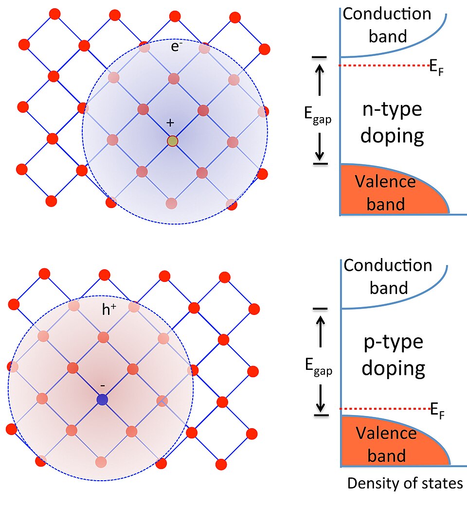 A labelled diagram showing N-type and P-type semiconductors with their respective doping atoms and charge carriers. (Image: Tem5psu, CC BY-SA 4.0, via Wikimedia Commons)
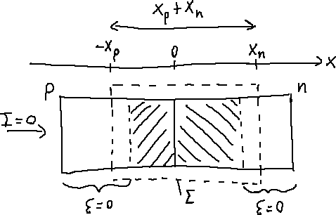 A diagram showing the depletion region in a PN junction under forward and reverse bias. (Image: Luca Ghio, CC BY-SA 3.0, via Wikimedia Commons)
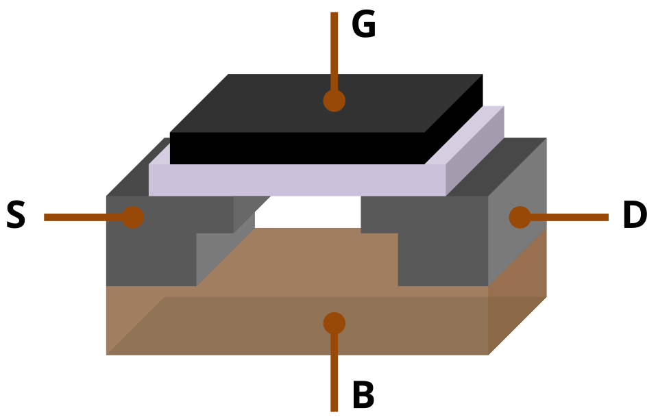 A cross-sectional diagram of an N-channel MOSFET showing source, gate, and drain terminals. (Image: Original: Brews ohare Vector: BentSm, CC BY-SA 3.0, via Wikimedia Commons)
Based on the NEB +2 Science syllabus for Physics (Phy), unit 24.
Discussion
Loading…