Electronic Devices and CircuitsUnit 711 min read
FETs: Types, Working, Biasing & Applications
Unit 7 of Electronic Devices and Circuits covers JFETs, MOSFETs, and their biasing techniques, including transfer characteristics, small-signal models, and real-world applications in amplifiers, switches, and digital circuits. Learn how FETs differ from BJTs, their pinch-off, threshold voltage, and amplification roles,
Key Concepts & Structure
Field Effect Transistors (FETs) are voltage-controlled devices where the input current is negligible (unlike BJTs). They are classified into:
- Junction Field Effect Transistor (JFET)
- Metal-Oxide-Semiconductor FET (MOSFET)
- Enhancement-mode MOSFET
- Depletion-mode MOSFET
We will explore:
- Construction & working principle (channel formation, pinch-off)
- Characteristics curves (drain, transfer)
- Biasing techniques (self-bias, voltage-divider bias)
- Small-signal models (hybrid-π equivalent)
- Applications (amplifiers, switches, memory cells)
- Comparison with BJTs
1. Construction & Working Principle
1.1 JFET Structure
A JFET has:
- A semiconductor channel (N-channel or P-channel)
- A gate (P-type for N-channel JFET, N-type for P-channel JFET)
- Source (S) and Drain (D) terminals
graph LR
    A["N-channel JFET"] --> B["N-type Semiconductor Channel"]
    A --> C["P-type Gate"]
    B --> D["Source (S)"]
    B --> E["Drain (D)"]
    C -->|"Reverse-biased"| F["Depletion Region"]
    F -->|"Pinches off channel"| G["Current Flow"]
How it works:
- A reverse bias is applied to the gate, creating a depletion region that narrows the channel.
- As gate voltage becomes more negative (for N-channel), the channel pinches off at (pinch-off voltage).
- Drain current is controlled by , not .
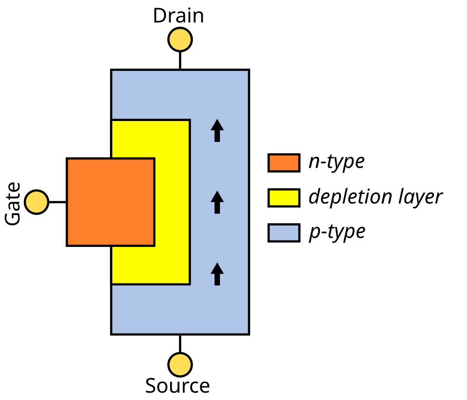 N-channel JFET showing gate, source, drain, and depletion region. (Image: Vector version: VectorVoyager PNG version: Rparle at English, CC BY-SA 3.0, via Wikimedia Commons)
1.2 MOSFET Structure
MOSFETs have an insulated gate (SiO₂ layer), making them input-current-free and ideal for digital circuits.
graph LR
    A["N-channel Enhancement MOSFET"] --> B["N-type Substrate"]
    A --> C["P-type Well"]
    A --> D["SiO2 Insulator"]
    A --> E["Gate (Metal/Aluminum)"]
    C --> F["Source (S) & Drain (D)"]
    E -->|"Positive V_GS"| G["Inversion Layer"]
    G -->|"Forms channel"| H["Current Flow"]
Types of MOSFETs:
| Type | Symbol | Channel Formation | Key Feature |
|---|---|---|---|
| Enhancement-mode | ![Enhancement MOSFET] | No channel at ; forms when | Used in digital logic (CMOS) |
| Depletion-mode | ![Depletion MOSFET] | Channel exists at ; can be enhanced or depleted | Rare, used in analog circuits |
2. Characteristics Curves
2.1 Drain Characteristics ( vs )
For a fixed :
- Cutoff region: (channel not pinched)
- Triode (ohmic) region: increases, increases linearly
- Saturation (active) region: Channel pinches off; saturates
2.2 Transfer Characteristics ( vs )
For JFET: where:
- = Drain current at
- = Pinch-off voltage
For Enhancement MOSFET: where is the process transconductance parameter.
3. Biasing Techniques
Proper biasing ensures the FET operates in the active region for linear amplification.
3.1 Self-Bias (Most Common for JFET)
- Uses a source resistor to set .
- Advantages: Simple, stable against temperature variations.
- Disadvantage: Lower gain due to .
Circuit:
graph LR
    A["V_DD"] --> B["Drain"]
    B --> C["R_D"]
    C --> D["Drain Terminal"]
    D --> E["Load"]
    D --> F["Ground"]
    G["Source"] --> H["R_S"]
    H --> I["Ground"]
    J["Gate"] --> K["Ground via R_G (optional)"]
Worked Example (Self-Bias for JFET): Given:
- , ,
- ,
Find and :
- Assume initially.
- .
- Use transfer characteristic equation:
- Solve iteratively (or use graph) to find , .
Real-World Tie-In: In NTC’s power amplifiers, JFETs are self-biased to ensure stable operation across varying loads (e.g., speakers).
3.2 Voltage-Divider Bias (MOSFET)
- Uses a resistor network to set .
- Advantage: More stable than self-bias for MOSFETs.
Circuit:
graph LR
    A["V_DD"] --> B["R1"]
    B --> C["Gate"]
    C --> D["R2"]
    D --> E["Ground"]
    F["Drain"] --> G["R_D"]
    G --> H["Ground"]
    I["Source"] --> J["R_S"]
    J --> K["Ground"]
Worked Example (Voltage-Divider Bias for MOSFET): Given:
- , ,
- ,
Find and :
Real-World Tie-In: Khalti’s payment processing circuits use MOSFETs in voltage-divider bias to ensure stable gate voltages for high-speed switching in payment gateways.
4. Small-Signal Model (Hybrid-π Equivalent)
For AC analysis, FETs are modeled as:
- JFET/MOSFET:
- Transconductance
- Output resistance (Early effect)
- Gate-source capacitance
Small-Signal Model:
graph LR
    A["V_gs"] --> B["g_m"]
    B --> C["I_d"]
    D["V_ds"] --> E["r_o"]
    E --> C
    F["C_gs"] -->|"Capacitor"| G["Gate to Source"]
    H["C_ds"] -->|"Capacitor"| I["Drain to Source"]
Calculating : For JFET: For MOSFET (enhancement):
Worked Example: Given , , :
5. Applications of FETs
| Application | FET Type | Why FET? | Example |
|---|---|---|---|
| Amplifiers | JFET, MOSFET | High input impedance, low noise | Ncell’s RF amplifiers |
| Switching | MOSFET | Fast switching, low power loss | Daraz’s power supply circuits |
| Digital Logic (CMOS) | Enhancement MOSFET | Low power, high density | Microcontrollers in eSewa apps |
| Voltage-Controlled Resistor | JFET | Variable resistance with | Automatic brightness control |
6. Comparison: FET vs BJT
| Parameter | FET | BJT |
|---|---|---|
| Control | Voltage-controlled | Current-controlled |
| Input Impedance | Very high (~10¹² Ω) | Low (~1kΩ) |
| Noise | Lower | Higher |
| Thermal Stability | Better (no minority carriers) | Worse (thermal runaway risk) |
| Switching Speed | Faster (MOSFET) | Slower |
| Applications | Digital logic, RF, amplifiers | Analog amplifiers, switches |
7. Common Mistakes & Exam Tips
Mistakes to Avoid:
- Confusing (JFET) and (MOSFET):
- is for JFET (pinch-off voltage).
- is for MOSFET (threshold voltage).
- Ignoring the saturation region in biasing calculations.
- Assuming MOSFETs work like JFETs (e.g., depletion vs enhancement modes).
- Forgetting the Early effect () in small-signal models.
Exam Tips:
- Always check the region of operation (cutoff, triode, saturation).
- Memorize the transfer characteristic equations for JFET and MOSFET.
- Practice biasing circuits—examiners love numerical problems!
- Compare FET and BJT in terms of input impedance, noise, and applications.
- For MOSFETs, distinguish between enhancement and depletion modes.
Real Exam Question Example: "A JFET has and . If , find and the small-signal transconductance ." Solution:
- Use .
- .
In the Real World
Ncell’s Base Stations
- What? RF amplifiers use MOSFETs (e.g., GaN HEMTs) for high-frequency signal boosting.
- Why FET? High efficiency, low distortion, and ability to handle high power at microwave frequencies.
eSewa’s Payment Processing
- What? MOSFETs in switching regulators (e.g., buck converters) for efficient power conversion.
- Why FET? Fast switching reduces power loss; enhancement-mode MOSFETs are used for digital control signals.
Daraz’s Warehouse Automation
- What? JFET-based sensors detect inventory levels (e.g., load cells with JFET amplifiers).
- Why FET? High input impedance prevents loading effects on sensitive sensors.
NTC’s Traffic Light Controllers
- What? CMOS logic (FETs) controls timing sequences.
- Why FET? Low power consumption and noise immunity in outdoor environments.
Khalti’s Security Chips
- What? MOSFET-based EEPROM stores encryption keys.
- Why FET? Non-volatile memory with high density and low power.
Summary Table for Quick Revision
| Topic | Key Formula/Concept | Real-World Link |
|---|---|---|
| JFET Transfer Char. | NTC amplifiers | |
| MOSFET Transfer Char. | Khalti payment circuits | |
| Self-Bias | Daraz power supplies | |
| Small-Signal | (MOSFET) | Ncell RF amplifiers |
| Pinch-Off | JFET switches in sensors |
Final Note: FETs are ubiquitous in modern electronics due to their efficiency, speed, and scalability. Master biasing, small-signal models, and comparisons with BJTs—these are high-weightage topics in exams. Always draw the circuit before solving numerical problems!
Based on the PU BE Computer (PU) syllabus for Electronic Devices and Circuits (ELX120), unit 7.
Discussion
Loading…