Electronic Devices and CircuitsUnit 86 min read
Small-Signal Amplifiers: Configurations, Analysis & Design
Unit 8 of Electronic Devices and Circuits explores small-signal amplifiers, covering their configurations (CE, CB, CC), frequency response, hybrid-π model, and design considerations for voltage/current gain, bandwidth, and stability. Includes real-world applications, worked examples, and exam-focused tips.
Key Concepts and Configurations
Small-signal amplifiers amplify weak AC signals (e.g., audio, sensor outputs) while ignoring DC components. They are analyzed using small-signal models (hybrid-π for BJTs, simplified models for FETs) and classified by transistor configuration:
1. Amplifier Configurations
Three basic configurations determine input/output impedance, gain, and stability:
| Configuration | Input Impedance | Output Impedance | Voltage Gain () | Current Gain () | Applications |
|---|---|---|---|---|---|
| Common Emitter (CE) | Medium | Low | High (inverting) | High | Audio preamps, RF stages |
| Common Base (CB) | Low | High | High (non-inverting) | Low | High-frequency amplifiers |
| Common Collector (CC) | High | High | Unity (non-inverting) | High | Buffer/impedance matching |
Why it matters: CE is most common for general-purpose amplification; CB excels at high frequencies; CC is used for impedance matching.
2. Hybrid-π Small-Signal Model for BJTs
The hybrid-π model simplifies BJT analysis by replacing the transistor with equivalent resistors and controlled sources. Key components:
- : Input resistance (, where )
- : Transconductance ()
- : Output resistance (often ignored in low-frequency analysis)
graph LR
    A["V_in"] --> B["r_π"]
    B --> C["g_m"]
    C --> D["V_out"]
    B --> E["r_o"]
    E --> D
Worked Example: For a BJT with , , and :
Frequency Response and Bandwidth
Amplifiers have limited bandwidth due to parasitic capacitances (, ) and coupling capacitors. The frequency response is characterized by:
- Lower cutoff frequency (): Caused by coupling/emitter bypass capacitors.
- Upper cutoff frequency (): Caused by transistor junction capacitances.
- Bandwidth (): .
Bode Plot for CE Amplifier
Key Idea: The gain rolls off at below and above .
Design Considerations
1. Gain Calculation
For a CE amplifier with and : where .
Worked Example (Real-World Tie-In): In a Khalti payment app’s audio feedback system, a CE amplifier drives a small speaker. Given:
- , , .
- Calculate : (unity gain is achieved by adjusting or ).
2. Stability and Feedback
Negative feedback improves stability but reduces gain. Common feedback types:
- Voltage-series: Reduces output impedance, increases input impedance.
- Current-shunt: Increases output impedance, reduces input impedance.
In the Real World
Pathao’s Ride-Hailing App:
- Uses CE amplifiers in its GPS signal conditioning circuits to boost weak antenna signals before processing. The high gain of CE stages ensures accurate location data for driver matching.
Ncell’s Base Station Transmitters:
- CB amplifiers are employed in RF stages to amplify high-frequency signals (e.g., 4G/5G) with minimal distortion. Their low input impedance matches the antenna’s impedance for efficient power transfer.
eSewa’s Payment Terminals:
- CC (Emitter Follower) amplifiers buffer signals between the payment terminal’s ADC and the display driver. Their unity gain and high input impedance prevent loading effects on the ADC.
Exam Tip
Memorize Hybrid-π Parameters:
- , , . Always derive these from given data.
Configuration Trade-offs:
- CE: High gain, inverting.
- CB: High-frequency, non-inverting.
- CC: Unity gain, buffer. Exam Question: "Which config would you choose for a 100 MHz amplifier?" → CB (high ).
Frequency Response:
- Sketch the Bode plot for a given and . Label the points and roll-off rates.
Feedback Analysis:
- For a feedback amplifier, calculate the closed-loop gain using: .
- Identify if feedback is series/shunt and its effect on and .
Real-World Scenarios:
- Expect questions like: "Design a preamp for a Daraz delivery tracking sensor (output: 10 mV, )." → Use CE with , bias , and calculate .
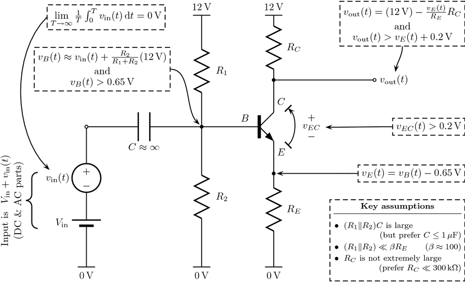 Labelled CE amplifier with , , and bias network. (Image: TedPavlic, CC BY-SA 3.0, via Wikimedia Commons)
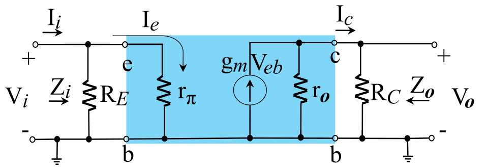 Hybrid-π model with , , and . (Image: Michel Bakni, CC BY-SA 4.0, via Wikimedia Commons)
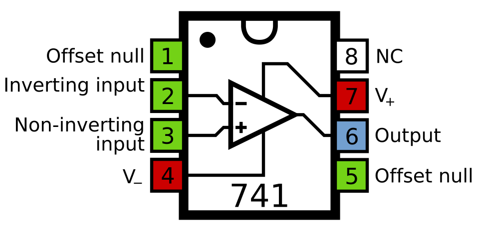 Real OP-AMP chip (741) for comparison with discrete amplifiers. (Image: Inductiveload, Public domain, via Wikimedia Commons)
Based on the PU BE Computer (PU) syllabus for Electronic Devices and Circuits (ELX120), unit 8.
Discussion
Loading…