Applied PhysicsUnit 99 min read
Semiconductor Physics – Band Theory, Doping, Devices, and Applications
Unit 9 of Applied Physics: covers semiconductor fundamentals, band structure, intrinsic/extrinsic behavior, carrier dynamics, p‑n junctions, diodes, BJTs, MOSFETs, and real‑world applications in electronics.
Key points
- Semiconductors have a band gap that allows control of electrical conductivity.
- Doping introduces donor or acceptor levels, creating n‑type or p‑type material.
- Carrier concentration and mobility determine conductivity and temperature dependence.
- p‑n junctions form the basis of diodes, transistors, and integrated circuits.
- MOSFETs and BJTs are the two dominant transistor technologies in modern electronics.
Introduction
Semiconductors are the backbone of modern electronics. Unlike conductors, whose electrons are free, or insulators, whose electrons are tightly bound, semiconductors possess a band gap that can be manipulated to control charge transport. This unit explains the physics behind that control, the creation of p‑type and n‑type materials, and how these materials combine to form the devices that power smartphones, computers, and power grids.
Band Theory of Solids
In a crystalline solid, atomic orbitals overlap to form energy bands. The valence band is filled with electrons, while the conduction band is typically empty. The energy difference between the top of the valence band and the bottom of the conduction band is the band gap .
- Metals: – valence and conduction bands overlap.
- Insulators: eV – very few electrons can be thermally excited.
- Semiconductors: eV – moderate excitation possible.
The probability that an electron occupies an energy level at temperature follows the Fermi‑Dirac distribution:
where is the Fermi level and is Boltzmann’s constant.
Merkle Diagram: Band Structure Flow
flowchart TD
  "Atomic Orbitals" --> "Overlap → Energy Bands"
  "Energy Bands" --> "Valence Band"
  "Energy Bands" --> "Conduction Band"
  "Band Gap" --> "Control of Conductivity"
Intrinsic Semiconductors
An intrinsic semiconductor is pure, with no intentional impurities. At absolute zero, all electrons occupy the valence band. As temperature rises, electrons acquire enough thermal energy to cross the band gap, leaving behind holes in the valence band.
The intrinsic carrier concentration is given by:
where and are the effective density of states in the conduction and valence bands, respectively.
Worked Example – Silicon at 300 K
- eV
Thus, intrinsic silicon at room temperature has about electrons and an equal number of holes per cubic centimeter.
Extrinsic Semiconductors and Doping
To achieve useful conductivity, semiconductors are doped with impurities that introduce energy levels close to the band edges.
| Dopant | Donor/Acceptor | Energy Level | Resulting Type |
|---|---|---|---|
| Phosphorus, Arsenic, Antimony | Donor | Near conduction band | n‑type |
| Boron, Aluminum, Gallium | Acceptor | Near valence band | p‑type |
n‑Type Doping
Adding a group‑V element (e.g., phosphorus) contributes an extra valence electron. This electron occupies a donor level just below the conduction band, making it easy to excite into the conduction band.
- Electron concentration (donor concentration).
- Hole concentration .
p‑Type Doping
Adding a group‑III element (e.g., boron) creates an acceptor level just above the valence band, effectively generating holes.
- Hole concentration (acceptor concentration).
- Electron concentration .
Mermaid Diagram: Doping Process
flowchart LR
  "Silicon Crystal" --> "Introduce Dopant"
  "Introduce Dopant" --> "Create Donor Level"
  "Introduce Dopant" --> "Create Acceptor Level"
  "Donor Level" --> "n‑type Conductivity"
  "Acceptor Level" --> "p‑type Conductivity"
Carrier Concentration and Conductivity
Electrical conductivity in a semiconductor is:
where is the elementary charge, and are electron and hole mobilities.
- Mobility depends on scattering mechanisms (phonon, impurity).
- In n‑type material, .
- In p‑type material, .
Temperature Dependence
- Intrinsic: – increases rapidly with .
- Extrinsic: At low , carriers freeze out; at moderate , conductivity rises linearly with due to increased carrier concentration; at high , mobility decreases due to phonon scattering.
Graph: Conductivity vs Temperature for intrinsic and extrinsic silicon
p‑n Junctions
A p‑n junction is formed by joining p‑type and n‑type regions. At the interface, electrons diffuse from n to p, and holes diffuse from p to n, creating a depletion region with an internal electric field.
- Built‑in potential .
- Depletion width .
Diode I‑V Characteristic
The Shockley equation describes the current:
where is the saturation current.
Worked Example – Silicon Diode
- , , .
- .
Bipolar Junction Transistors (BJTs)
A BJT consists of two p‑n junctions: emitter–base (EB) and base–collector (BC). There are two types: NPN and PNP.
- Current gain .
- Collector current (for active region).
NPN Operation
- Forward‑active: EB junction forward‑biased, BC junction reverse‑biased.
- Saturation: Both junctions forward‑biased.
- Cut‑off: Both junctions reverse‑biased.
Mermaid Diagram: BJT Operation Modes
stateDiagram-v2
  [*] --> ForwardActive : EB forward, BC reverse
  ForwardActive --> Saturation : EB & BC forward
  ForwardActive --> Cutoff : EB & BC reverse
Metal‑Oxide‑Semiconductor Field‑Effect Transistors (MOSFETs)
MOSFETs control current via an electric field applied to a gate electrode separated by an oxide layer.
- Types: Enhancement‑mode (normally off) and depletion‑mode (normally on).
- Key parameters: Threshold voltage , transconductance , drain current .
Enhancement‑Mode nMOSFET Current Equation
where and are channel width and length, is oxide capacitance per unit area.
Worked Example – nMOSFET
- , , , , .
- For :
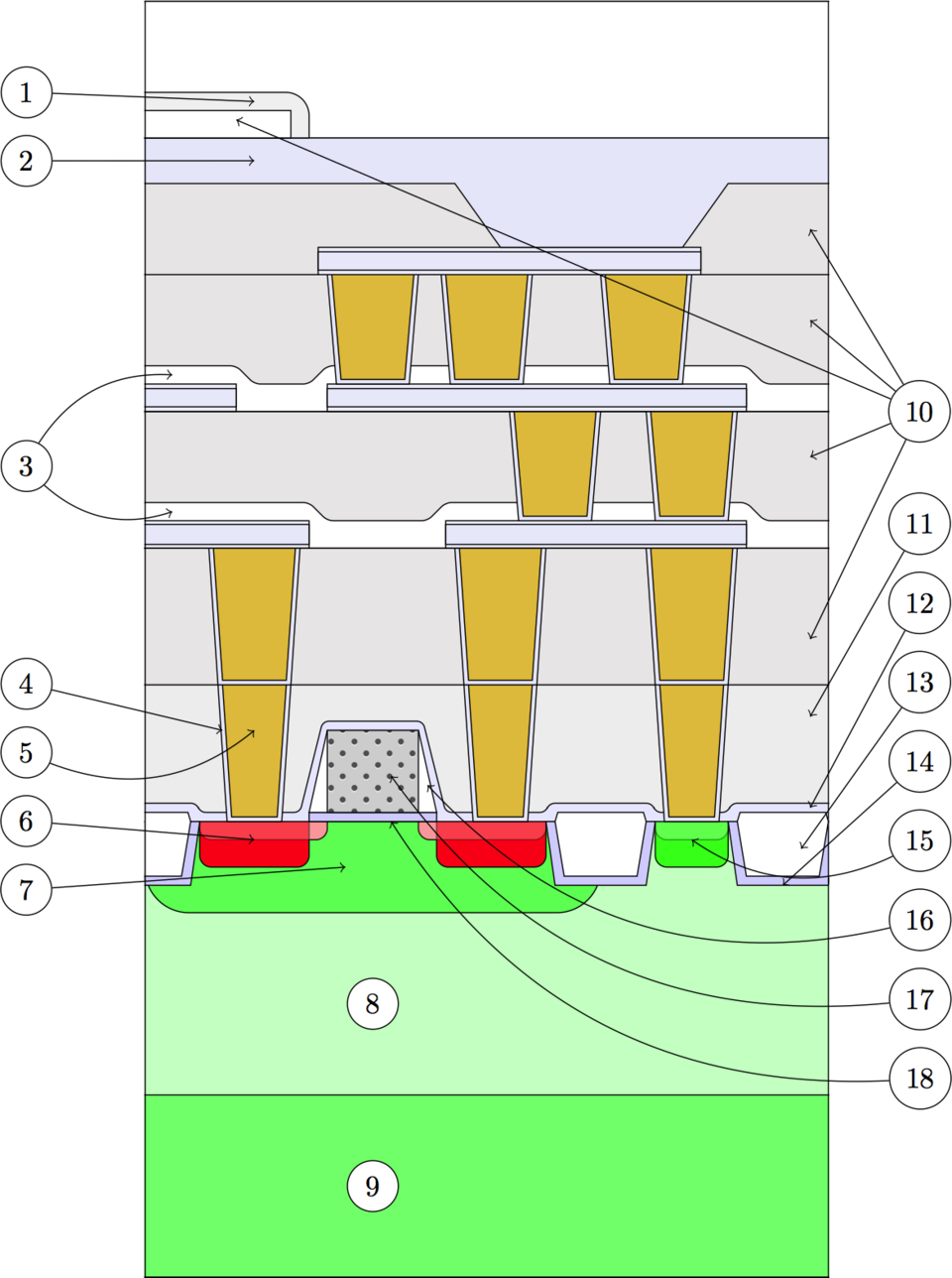 Cross‑section of an nMOSFET showing gate oxide and channel (Image: Vegar Ottesen, CC BY-SA 3.0, via Wikimedia Commons)
Applications
| Device | Application | Key Semiconductor Concept |
|---|---|---|
| Diode | Rectifiers in power supplies | p‑n junction, forward bias |
| BJT | Amplifiers in audio circuits | current gain, transistor operation |
| MOSFET | Logic gates in CPUs | field‑effect control, scaling |
| Solar cell | Photovoltaic panels | p‑n junction, built‑in field |
| LED | Display backlights | direct band‑gap recombination |
In the real world
- eSewa uses MOSFET‑based power management ICs to regulate the voltage supplied to its servers, ensuring efficient data handling.
- Daraz relies on silicon‑based BJT switches in its warehouse automation robots for precise motion control.
- Ncell’s base stations incorporate high‑power MOSFETs to amplify RF signals, demonstrating the importance of carrier mobility and thermal management.
In the real world
- Google Search Engine – Uses billions of MOSFETs in its data centers to switch and amplify signals, directly applying the field‑effect principle.
- Pathao Delivery App – Relies on embedded microcontrollers with silicon BJTs for sensor interfacing and power regulation.
- NEPSE Trading Platform – Employs high‑speed silicon photodiodes (p‑n junctions) for optical data links, showcasing the role of semiconductor physics in financial infrastructure.
Exam tip
- Understand the derivation of key equations (e.g., , for MOSFETs).
- Practice numerical problems: carrier concentration, depletion width, and I‑V curves.
- Draw band diagrams for intrinsic, n‑type, and p‑type semiconductors; label donor/acceptor levels.
- Know the differences between BJT and MOSFET operation modes and their characteristic curves.
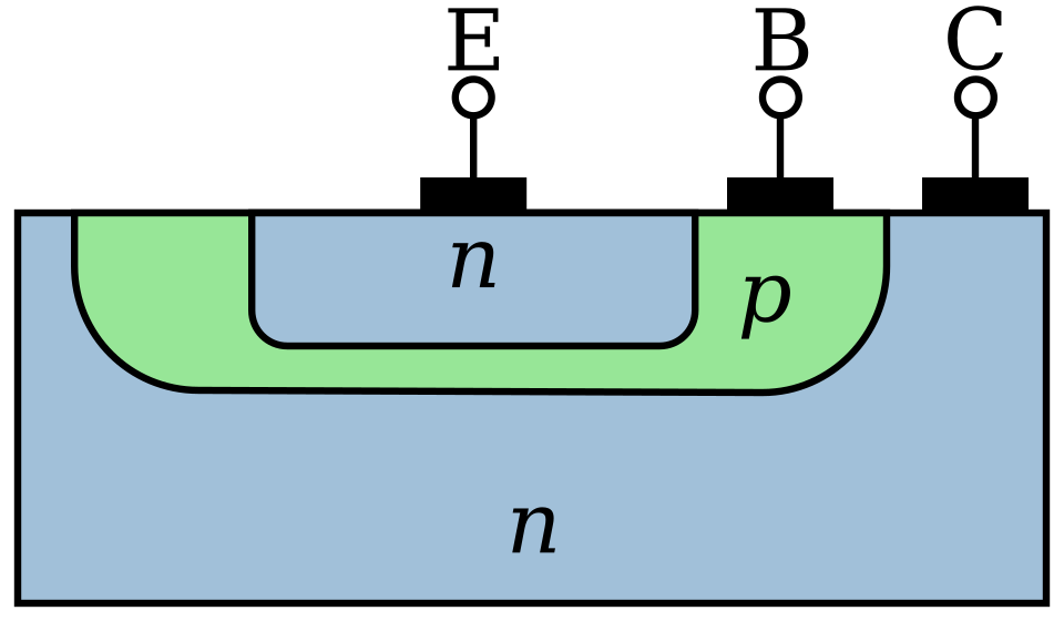 Detailed cross‑section of a BJT with doping profiles (Image: Inductiveload, Public domain, via Wikimedia Commons)
Detailed cross‑section of a MOSFET showing gate oxide and channel (Image: Vegar Ottesen, CC BY-SA 3.0, via Wikimedia Commons)
Based on the PU BE Computer (PU) syllabus for Applied Physics, unit 9.
Discussion
Loading…