Embedded SystemUnit 49 min read
Embedded Memory & Interfacing: Types, Protocols & Design
Unit 4 of Embedded System explores memory hierarchies (RAM, Flash, EEPROM), interfacing techniques (parallel/serial), bus architectures (address/data buses), and real-world applications like sensor data logging and IoT device communication.
Core Concepts
Memory in Embedded Systems
Embedded systems rely on limited memory compared to general-purpose computers. Memory types are categorized by speed, volatility, and cost:
classDiagram
    class Memory {
        <<abstract>>
        +speed: ms/ns
        +volatility: volatile/non-volatile
        +cost: low/medium/high
    }
    class RAM {
        +volatile
        +fast access
        +used for runtime data
    }
    class Flash {
        +non-volatile
        +slower than RAM
        +used for firmware storage
    }
    class EEPROM {
        +non-volatile
        +byte-level writable
        +used for configuration
    }
    Memory <|-- RAM
    Memory <|-- Flash
    Memory <|-- EEPROM
Key Memory Types in Embedded Systems
| Type | Volatility | Speed | Use Case | Example (8-bit MCU) |
|---|---|---|---|---|
| SRAM | Volatile | Fastest | Runtime variables, stack, heap | 8051’s internal SRAM (128B) |
| Flash | Non-volatile | Medium | Firmware storage (bootloader, code) | 256KB–1MB external Flash |
| EEPROM | Non-volatile | Slow | Configuration (e.g., sensor calib.) | 256B–4KB internal EEPROM |
| FRAM | Non-volatile | Fast (like SRAM) | Real-time logging (e.g., GPS data) | FM24CL64 (64KB FRAM) |
Memory Interfacing Techniques
Embedded systems interface memory using address/data buses and control signals. Two primary methods:
Parallel Interfacing
- Uses multiple data lines (e.g., 8-bit or 16-bit buses).
- Faster but requires more pins.
- Example: Connecting an external SRAM (6116) to an 8051.
flowchart TD A["8051 MCU"] -->|"AD0-AD7"| B["6116 SRAM Data Bus"] A -->|"A8-A15"| C["6116 Address Bus"] A -->|"RD"| D["6116 Read Enable"] A -->|"WR"| E["6116 Write Enable"] - Worked Example: Interfacing 256KB Flash (27C256) with an 8051.
- Address Lines: A0–A17 (18 lines for 262,144 bytes).
- Data Lines: D0–D7 (8-bit bus).
- Control Signals: OE (Output Enable), CE (Chip Enable).
- Calculation: For 256KB, bytes → 18 address lines needed.
Serial Interfacing
- Uses SPI/I2C for slower but pin-efficient communication.
- Example: 24LC256 EEPROM (256KB) over I2C.
flowchart TD A["MCU"] -->|"SDA"| B["24LC256 EEPROM"] A -->|"SCL"| B A -->|"SDA"| C["Pull-up Resistors"] A -->|"SCL"| C - Advantages: Fewer pins, longer cable lengths.
- Disadvantages: Slower than parallel.
Bus Architectures
Embedded systems use shared buses for communication between CPU, memory, and peripherals. Key buses:
| Bus Type | Lines | Function | Example |
|---|---|---|---|
| Address Bus | A0–A15 (8051) | Selects memory/peripheral location | 8051’s P0–P2 (multiplexed) |
| Data Bus | D0–D7 (8-bit) | Transfers data | 8051’s P0 port |
| Control Bus | RD, WR, RESET, ALE | Manages read/write operations | 8051’s control signals |
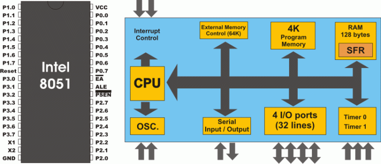 Highlights address/data buses and control signals. (Image: Microe, Public domain, via Wikimedia Commons)
Real-World Applications
1. eSewa (Nepal) – Secure Transaction Logging
- Idea Used: EEPROM for non-volatile transaction storage.
- How: When you pay utility bills via eSewa, the app logs your transaction details (amount, time, merchant ID) in internal EEPROM of the payment gateway’s MCU. This ensures data persists even if power is lost.
- Why EEPROM?
- Non-volatile → survives power cycles.
- Byte-writable → updates individual records without rewriting the entire memory.
2. Pathao Driver App – Real-Time Route Optimization
- Idea Used: FRAM for high-speed GPS data logging.
- How: Pathao’s backend uses FRAM-based loggers in IoT devices to record driver locations in real-time. Unlike Flash, FRAM allows millions of write cycles without degradation, critical for continuous GPS updates.
- Worked Example:
- A Pathao driver’s MCU logs coordinates every second.
- Memory Calculation: If each log is 16 bytes (latitude, longitude, timestamp), and the driver logs for 8 hours: .
- Solution: A 4MB FRAM (e.g., FM25V40) suffices, with fast read/write for real-time processing.
3. NTC Smart Meters – Firmware Updates via SPI Flash
- Idea Used: External SPI Flash for over-the-air (OTA) updates.
- How: NTC’s smart meters use SPI-connected Flash memory (e.g., W25Q128) to store firmware. When an update is pushed from the server, the meter’s MCU reads the new binary from Flash and executes it.
- Why SPI?
- 3-wire interface (SCLK, MOSI, MISO) reduces pin count.
- Faster than I2C for large firmware (e.g., 1MB+).
Memory Interfacing Worked Example: Interfacing ADC0804 with 8051
Problem: Connect an 8-bit ADC (ADC0804) to an 8051 to read analog sensor data (e.g., temperature).
flowchart TD
    A["8051 P1.0"] -->|"INTR"| B["ADC0804 INT"]
    A["P1.1"] -->|"WR"| C["ADC0804 WR"]
    A["P1.2"] -->|"RD"| D["ADC0804 RD"]
    A["P0"] -->|"D0-D7"| E["ADC0804 Data Bus"]
    A["P2.0"] -->|"ALE"| F["Address Latch"]
G["Sensor"] -->|"Vin"| H["ADC0804 Analog Input"]Steps:
- Connect Pins:
- Data Bus: P0 (8051) ↔ D0–D7 (ADC0804).
- Control Signals:
- P1.1 → WR (Write to ADC).
- P1.2 → RD (Read from ADC).
- P1.0 → INT (Conversion complete interrupt).
- Initialization:
- Send start conversion pulse on WR.
- Wait for INT signal (polling or interrupt-driven).
- Read Data:
- Pull RD low → ADC outputs 8-bit result on P0.
- Example Code (8051 Assembly):
MOV P1, #0x02   ; Set WR low (start conversion)
NOP
MOV P1, #0x03   ; Release WR
WAIT: JNB P1.0, WAIT  ; Wait for INT (conversion done)
MOV P1, #0x01   ; Set RD low to read data
MOV A, P0       ; Read 8-bit result into A
MOV P1, #0x03   ; Release RD
Real-World Tie-In:
- Nepal’s Air Quality Monitors: These use ADC0804 (or similar) to convert analog signals from CO₂, PM2.5 sensors into digital values for the MCU to process. The data is then logged to SD cards (via SPI) or sent to a cloud server.
Common Interfacing Protocols
1. UART (Asynchronous Serial)
- Use Case: Debugging (e.g., printing sensor data to PC via USB-to-UART).
- Example: Connecting an Arduino (ATmega328P) to a PC for serial monitoring.
flowchart TD
    A["PC USB"] -->|"UART"| B["FTDI Chip"]
    B -->|"TX/RX"| C["ATmega328P UART"]
2. SPI (Synchronous Serial)
- Use Case: High-speed peripherals (Flash, ADCs, sensors).
- Example: Interfacing MPU6050 (IMU sensor) with an STM32.
flowchart TD
    A["STM32"] -->|"SCLK"| B["MPU6050"]
    A -->|"MOSI"| B
    A -->|"MISO"| B
    A -->|"CS"| B
3. I2C (Inter-Integrated Circuit)
- Use Case: Multiple slow devices (EEPROM, RTC, LCD).
- Example: Connecting DS3231 RTC and 24LC256 EEPROM to an 8051.
flowchart TD
    A["8051"] -->|"SDA"| B["DS3231"]
    A -->|"SCL"| B
    A -->|"SDA"| C["24LC256"]
    A -->|"SCL"| C
Comparison Table:
| Protocol | Speed | Pins Used | Devices | Example Use Case |
|---|---|---|---|---|
| UART | 9600–115200 bps | 2 (TX, RX) | Single device | Debugging via PC |
| SPI | 1–50 Mbps | 4 (SCLK, MOSI, MISO, CS) | Single master, multiple slaves | Flash memory, ADCs |
| I2C | 100 kbps–4 Mbps | 2 (SDA, SCL) | Multiple devices | RTC, EEPROM, LCDs |
Exam Tip
- Memory Maps: Always draw the memory map for MCUs like 8051, showing:
- Internal RAM (128B for 8051).
- External memory (if used).
- Special function registers (SFRs).
- Address Calculation: For external memory (e.g., 64KB SRAM), calculate:
- Number of address lines needed: .
- Example: 64KB = 65,536 bytes → address lines.
- Interfacing Diagrams: In exams, always sketch the connection between MCU and peripheral, labeling:
- Data bus, address bus, control signals.
- Example: Show how an 8051 connects to 27C512 (256KB Flash) with A0–A17, D0–D7, and OE/CE.
- Protocol Differences: Know when to use UART (debugging), SPI (high-speed), or I2C (multi-device).
- Real-World Scenarios: Expect questions like:
- "Why does Pathao use FRAM instead of Flash for GPS logging?"
- "How would you interface a temperature sensor (LM35) to an 8051?" (Answer: ADC + parallel/SPI bus).
- Common Pitfalls:
- Forgetting address latch enable (ALE) in 8051’s multiplexed buses.
- Misconfiguring chip select (CS) for SPI/I2C devices.
- Not accounting for memory bank switching in 8051’s external memory.
Based on the PU BE Computer (PU) syllabus for Embedded System (ELX320), unit 4.
Discussion
Loading…