Microprocessor and Computer ArchitectureUnit 18 min read
Microprocessors, Architecture & Computer Systems: Basics
Unit 1 of Microprocessor and Computer Architecture introduces the core concepts of microprocessors, their role in computer systems, and the fundamental architecture that powers modern computing—from smartphones to supercomputers. This note covers definitions, historical evolution, functional units, and real-world appli
What is a Microprocessor?
A microprocessor (or CPU) is the central processing unit of a computer, responsible for executing instructions, performing arithmetic/logic operations, and managing data flow. It is the "brain" of any digital device, from calculators to servers.
Key Components of a Microprocessor
classDiagram
class Microprocessor {
+ALU: Arithmetic Logic Unit
+CU: Control Unit
+Registers: Temporary storage (e.g., PC, IR, ACC)
+Cache: Fast memory (L1, L2)
+Clock: Synchronizes operations (GHz)
}
class ALU {
+Performs arithmetic (ADD, SUB)
+Performs logic (AND, OR, NOT)
}
class CU {
+Fetches instructions
+Decodes instructions
+Controls data flow
}
Microprocessor --> ALU : "Performs calculations"
Microprocessor --> CU : "Manages execution"
Microprocessor --> Registers : "Stores data temporarily"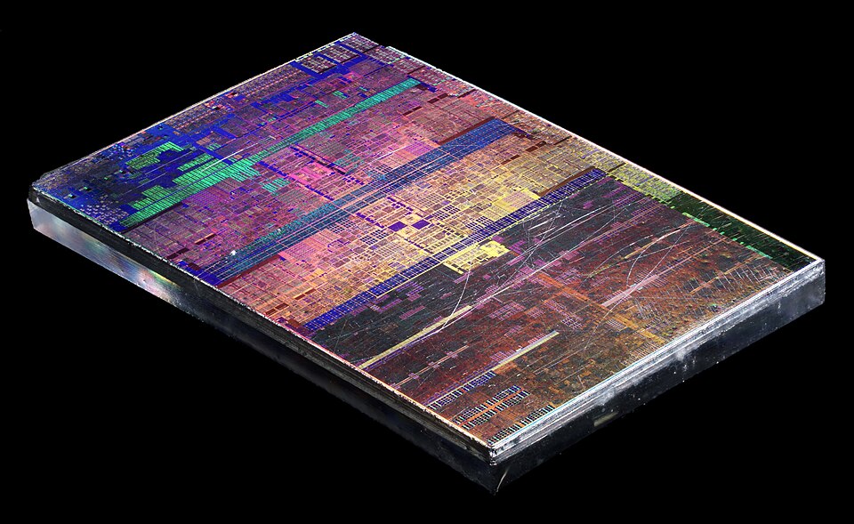 A close-up of a modern CPU showing its physical structure and transistor layout. (Image: Fritzchens Fritz from Berlin, CC0, via Wikimedia Commons)
How Microprocessors Work: The Fetch-Decode-Execute Cycle
Every instruction a microprocessor processes follows this 4-step cycle:
- Fetch: The Control Unit (CU) retrieves the next instruction from memory (RAM) using the Program Counter (PC).
- Decode: The Instruction Register (IR) holds the instruction, and the CU determines what operation to perform.
- Execute: The Arithmetic Logic Unit (ALU) or other units carry out the operation (e.g., addition, data transfer).
- Store: The result is written back to a register or memory.
Worked Example: Adding Two Numbers (A = 5, B = 3)
Assume the instruction ADD A, B is stored at memory address 0x1000.
Step 1: Fetch → PC = 0x1000 → Instruction = ADD A, B
Step 2: Decode → CU identifies "ADD" operation
Step 3: Execute → ALU computes 5 + 3 = 8
Step 4: Store → Result (8) saved in ACC (Accumulator)
Computer Architecture: The Big Picture
Computer architecture defines how hardware components (CPU, memory, I/O) interact. It is divided into two main models:
1. Von Neumann Architecture (Stored-Program Concept)
- Invented by: John von Neumann (1945)
- Key Idea: Program instructions and data are stored in the same memory.
- Components:
- CPU (ALU, CU, Registers)
- Memory (RAM, ROM)
- Input/Output (I/O) Units
- Data & Address Bus (for communication)
classDiagram
class VonNeumannArchitecture {
+CPU: Central Processing Unit
+Memory: Stores data & instructions
+I/O: Input/Output devices
+Bus: Data, Address, Control
}
class CPU {
+ALU: Arithmetic/Logic
+CU: Control
+Registers: Temporary storage
}
CPU --> Memory : "Fetches instructions"
CPU --> I/O : "Handles data transfer"
Memory --> Bus : "Sends/receives data"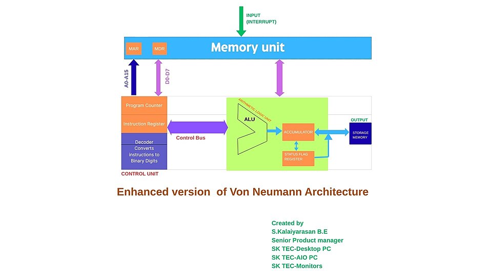 A labeled diagram showing CPU, memory, and I/O connections. (Image: SKTEC1977, CC BY 4.0, via Wikimedia Commons)
2. Harvard Architecture (Separate Data & Instruction Memory)
- Used in: Microcontrollers (e.g., Arduino, 8051), DSPs
- Key Idea: Separate memory buses for instructions and data → faster execution.
- Advantages:
- No von Neumann bottleneck (memory contention).
- Enables pipelining (overlapping fetch/decode/execute).
- Disadvantages:
- More expensive (dual memory).
- Less flexible (harder to modify programs at runtime).
| Feature | Von Neumann | Harvard |
|---|---|---|
| Memory Access | Shared bus for data & code | Separate buses for data & code |
| Speed | Slower (bottleneck) | Faster (parallel access) |
| Cost | Lower | Higher |
| Examples | x86 (Intel/AMD), ARM | AVR, PIC, TI DSPs |
## In the real world
eSewa (Nepal’s Digital Payment System)
- Idea Used: Von Neumann Architecture in servers processing transactions.
- How? When you pay bills via eSewa, the server’s CPU fetches your account details, decodes the payment instruction, executes the deduction, and stores the result—all following the fetch-decode-execute cycle.
Khalti (Mobile Banking App)
- Idea Used: Harvard Architecture in mobile processors (e.g., Qualcomm Snapdragon).
- How? The phone’s CPU separates instruction memory (app code) from data memory (your transaction details), allowing faster app responses during payments.
NTC’s Traffic Management System (Kathmandu)
- Idea Used: Microprocessor-based controllers (e.g., Raspberry Pi + sensors).
- How? Traffic lights use embedded microprocessors to fetch sensor data (car presence), decode timing rules, and execute light changes—all in real-time loops.
Types of Microprocessors
Microprocessors vary by bit-length (word size), architecture (CISC/RISC), and application.
Classification by Word Size
| Word Size | Examples | Use Cases |
|---|---|---|
| 8-bit | Intel 8085, PIC16F877 | Embedded systems (microwaves, toys) |
| 16-bit | Intel 8086, Zilog Z80 | Early PCs, gaming consoles |
| 32-bit | Intel Pentium, ARM Cortex-A9 | Laptops, smartphones (mid-2000s) |
| 64-bit | Intel Core i7, ARM Cortex-A72 | Modern PCs, servers, high-end phones |
Classification by Application
| Type | Examples | Key Feature |
|---|---|---|
| General-Purpose | Intel Core i7, AMD Ryzen | High performance, multitasking |
| Embedded | ARM Cortex-M, AVR ATmega328P | Low power, real-time control |
| Digital Signal Processing (DSP) | TI TMS320C674x | Optimized for audio/video processing |
| Graphics (GPU) | NVIDIA GeForce, AMD Radeon | Parallel processing for rendering |
How Microprocessors Interact with Other Components
A microprocessor does not work alone—it relies on supporting hardware for full functionality.
1. Memory Hierarchy
Microprocessors use a multi-level memory system to balance speed and cost.
stateDiagram-v2
    [*] --> Registers: "Fastest (ns access)"
    Registers --> Cache_L1: "KB-sized, ultra-fast"
    Cache_L1 --> Cache_L2: "MB-sized, slightly slower"
    Cache_L2 --> RAM: "GB-sized, slower (µs access)"
    RAM --> HDD/SSD: "TB-sized, slowest (ms access)"
2. Input/Output (I/O) Interfacing
Microprocessors communicate with peripherals (keyboard, screen, USB) via:
- Ports: Parallel (old printers), Serial (USB, UART).
- Interrupts: Signals from devices (e.g., keyboard press) to stop current task and handle I/O.
- DMA (Direct Memory Access): Allows devices (e.g., hard drives) to transfer data without CPU intervention.
Worked Example: Keyboard Input
- You press a key → keyboard controller sends an interrupt signal to the CPU.
- CPU saves its state, jumps to the Interrupt Service Routine (ISR).
- ISR reads the key code from the keyboard buffer.
- CPU restores state and resumes normal execution.
## Exam Tip
This unit is conceptual but heavily tested in TU exams. Expect:
- Definitions: Be ready to explain microprocessor, von Neumann architecture, and Harvard architecture with diagrams.
- Fetch-Decode-Execute Cycle: Draw the cycle and trace a simple instruction (e.g.,
MOV A, B). - Comparisons: Know the pros/cons of von Neumann vs. Harvard (speed, cost, flexibility).
- Real-World Applications: Link concepts to eSewa, Khalti, or traffic systems (e.g., "How does a microprocessor handle a Khalti payment?").
- Diagrams: Always label components in architecture diagrams (CPU, memory, buses).
- Short Questions: Practice 1-mark definitions (e.g., "What is an ALU?") and 5-mark explanations (e.g., "Compare 8-bit and 32-bit processors").
Common Mistakes to Avoid:
- Confusing Harvard and von Neumann architectures.
- Forgetting to include all 4 steps in the fetch-decode-execute cycle.
- Drawing unlabeled diagrams (examiners deduct marks for this!).
Based on the TU BIM syllabus for Microprocessor and Computer Architecture (IT236), unit 1.
Discussion
Loading…