Microprocessor and Computer ArchitectureUnit 712 min read
Memory Hierarchy & Organization: Levels, Speed, and Trade-offs
Unit 7 of Microprocessor and Computer Architecture: explores how computers organize memory into a multi-level hierarchy (registers → cache → RAM → disk) to balance speed, cost, and capacity, explains memory mapping, addressing, and access times, and contrasts volatile vs. non-volatile storage with real-world examples l
TAKEAWAYS:
- Memory hierarchy prioritizes speed over cost by using smaller, faster layers (registers, cache) for hot data and larger, slower layers (disk) for cold data.
- Cache memory (L1, L2, L3) reduces CPU stalls by storing frequently accessed instructions/data, but requires associative mapping or set-associative schemes.
- Virtual memory extends RAM using disk (swap space) but introduces page faults, increasing latency.
- Memory-mapped I/O simplifies hardware access by treating peripherals as memory locations, unlike isolated I/O’s dedicated ports.
- DRAM vs. SRAM: DRAM is cheaper but slower (used in RAM), while SRAM is faster (used in cache) but consumes more power.
- Memory bandwidth (GB/s) and latency (ns) are critical for performance; pipelining and prefetching mitigate bottlenecks.
1. Memory Hierarchy: Why Multiple Layers?
Computers use a multi-level memory hierarchy to balance speed, cost, and capacity. The closer memory is to the CPU, the faster but more expensive it is. The goal is to minimize average access time while keeping costs low.
The Memory Hierarchy (From Fastest to Slowest)
figure: Memory Hierarchy
| Level       | Type          | Size (bits) | Speed (ns) | Cost (per bit) | Example Use Case                     |
|-------------|---------------|-------------|------------|----------------|-------------------------------------|
| Registers   | SRAM          | 32–64       | 0.1–1      | $$$$$$         | CPU registers (AX, BX, PC)         |
| L1 Cache    | SRAM          | KB–MB       | 1–5        | $$$$           | Frequently used instructions/data   |
| L2 Cache    | SRAM          | MB–16MB     | 5–20       | $$$            | Branch prediction, loop variables   |
| L3 Cache    | SRAM          | 16MB–100MB  | 20–50      | $$             | Shared across CPU cores            |
| Main RAM    | DRAM          | GB–TB       | 50–150     | $              | Running programs, OS data           |
| SSD         | Flash         | TB–PB       | 100K–1M    | $              | Boot OS, apps, user files           |
| HDD         | Magnetic      | PB+         | 10M–20M    | $              | Backups, large datasets             |
Why this hierarchy?
- Locality Principle: Programs access the same data repeatedly (temporal locality) or nearby data (spatial locality).
- Trade-off: Faster memory is smaller and expensive; slower memory is larger and cheap.
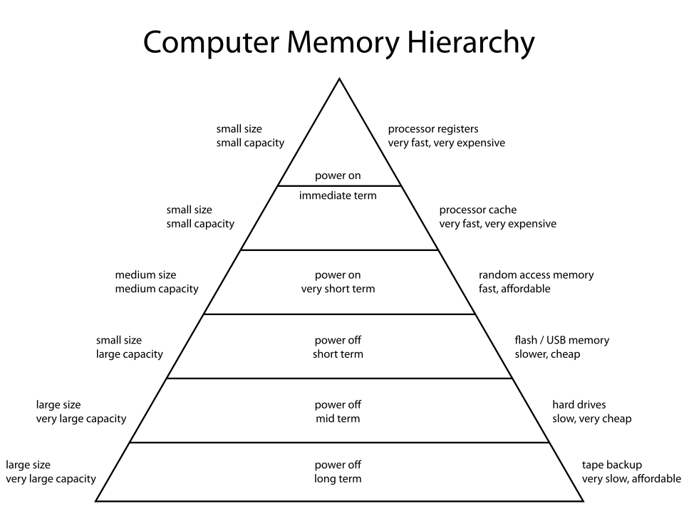 A layered cake of CPU registers (top), L1/L2/L3 cache, RAM, SSD, and HDD (bottom). (Image: ComputerMemoryHierarchy.png: User:Danlash at en.wikipedia.or, Public domain, via Wikimedia Commons)
2. Cache Memory: How It Works
Cache memory is a small, fast SRAM layer between the CPU and RAM. It stores copies of frequently used data to reduce access time.
Cache Organization
- Direct-Mapped Cache:
- Each memory block maps to one cache line.
- Simple but can cause conflicts (thrashing).
Example: If two blocks hash to the same line, the LRU (Least Recently Used) policy evicts the older one.
- Associative Cache:
- Any memory block can go to any cache line.
- No conflicts but slower (requires comparison).
- Set-Associative Cache (Most common):
- Cache divided into sets (e.g., 4-way set-associative).
- Each memory block maps to a set, not a single line.
Cache Hit/Miss
- Hit: Data is in cache → fast access (~1–5 ns).
- Miss: Data not in cache → RAM access (~50–150 ns).
- Miss Penalty: The time lost when cache misses occur.
Worked Example: Cache Hit/Miss Calculation
- Cache size: 16 KB, block size: 32 bytes.
- Access time: RAM = 100 ns, Cache = 5 ns.
- Hit rate: 90% (90% of accesses are cache hits).
- Average access time (AAT):
In the Real World:
- Ncell’s App Caching: When you open WhatsApp repeatedly, Ncell’s L3 cache stores the app’s binary to speed up launches.
- Google Chrome’s Disk Cache: Frequently visited websites (e.g., Daraz) are cached in SSD to reduce load times.
3. Main Memory (RAM): DRAM vs. SRAM
RAM is volatile (loses data when powered off) and used for active programs.
DRAM (Dynamic RAM)
- Cheaper, larger (used in main memory).
- Requires refreshing (every ~8 ms).
- Slower (~50–150 ns access time).
- IMAGE: "DRAM chip close-up" | A DRAM chip showing memory cells with capacitors.
SRAM (Static RAM)
- Faster, no refresh needed (used in cache).
- More power-hungry (6 transistors per bit vs. 1 in DRAM).
- IMAGE: "SRAM vs DRAM comparison" | A side-by-side of SRAM (top) and DRAM (bottom) cell structures.
Memory Addressing
- Linear Addressing: Each memory location has a unique address (e.g., 32-bit address bus → 4 GB RAM).
- Segmented Addressing: Divides memory into segments (e.g., code, data, stack).
- Paged Addressing: Uses pages (fixed-size blocks) for virtual memory.
Example: 32-bit Address Bus
- Address range: .
- If word size = 32 bits, then number of words = 4 GB / 4 bytes = 1 GB words.
4. Virtual Memory: Extending RAM with Disk
Virtual memory simulates more RAM than physically available by using disk (swap space).
How It Works
- Page Fault: CPU requests a page not in RAM → OS loads it from disk.
- Page Replacement: If RAM is full, the OS evicts a page (using algorithms like LRU, FIFO).
- Thrashing: Too many page faults → CPU spends more time waiting for disk than executing.
Page Replacement Algorithms
| Algorithm | Description | Example |
|---|---|---|
| FIFO | Replace oldest page | Not optimal for locality |
| LRU | Replace least recently used | Best for temporal locality |
| Optimal | Replace page not used for longest time | Impossible to implement |
| Clock | Circular buffer with "used" bit | Used in modern OS |
Worked Example: Page Fault Calculation
- RAM size: 4 pages, Disk access time: 10 ms, CPU time per page: 1 ms.
- Page reference string:
[1, 2, 3, 4, 1, 2, 5, 1, 2, 3, 4, 5] - Algorithm: LRU
- Page faults:
- Load 1, 2, 3, 4 → 4 faults.
- Replace 4 with 5 → 1 fault.
- Replace 3 with 1 → 1 fault.
- Total faults = 6.
- Total time:
In the Real World:
- NEPSE’s Market Data: When traders open NEPSE’s trading app, the OS pages in only the necessary market data into RAM, keeping other data on SSD to save space.
- Pathao’s Ride Booking: When you book a ride, Pathao’s backend caches frequently used driver locations in L3 cache to reduce latency.
5. Secondary Storage: SSD vs. HDD
Secondary storage is non-volatile (retains data when powered off).
| Feature | SSD (Solid State Drive) | HDD (Hard Disk Drive) |
|---|---|---|
| Technology | Flash memory (NAND) | Magnetic platters |
| Speed | 100K–1M IOPS | 50–200 IOPS |
| Latency | ~20–100 µs | ~5–10 ms |
| Reliability | No moving parts → more durable | Moving parts → prone to failure |
| Cost | $ (per GB) | $ (per GB) |
| Use Case | Boot OS, apps, databases | Backups, large files |
In the Real World:
- eSewa’s Transaction Logs: eSewa stores millions of transactions on SSDs for fast retrieval during audits.
- Daraz’s Order Database: Daraz uses HDDs for archived orders (cost-effective) and SSDs for active orders (fast access).
6. Memory-Mapped I/O vs. Isolated I/O
I/O devices (keyboard, disk) interact with the CPU via memory or dedicated ports.
| Feature | Memory-Mapped I/O | Isolated I/O |
|---|---|---|
| Address Space | Part of main memory | Dedicated I/O ports |
| Access Method | MOV AX, [0x200] |
IN AX, 0x200 |
| Simplicity | Easier (uses MOV) |
More complex (requires IN/OUT) |
| Speed | Faster (no port mapping) | Slower (extra cycle) |
| Use Case | Modern systems (PCIe) | Legacy systems (8085) |
Example: 8085 Microprocessor
- Isolated I/O: Uses
IN/OUTinstructions.IN AL, 0x20 ; Read from port 0x20 OUT 0x20, AL ; Write to port 0x20 - Memory-Mapped I/O: Treats I/O as memory.
MOV AL, [0x200]  ; Read from address 0x200
MOV [0x200], AL  ; Write to address 0x200
In the Real World:
- NTC’s Router Configuration: NTC’s routers use memory-mapped I/O to read/send network packets efficiently.
- Khalti’s Payment Gateway: When you pay via Khalti, the payment request is sent via memory-mapped I/O to the payment server.
7. DMA (Direct Memory Access)
DMA allows peripherals (disk, network card) to transfer data directly to/from RAM without CPU intervention.
How DMA Works
- CPU sends DMA request to peripheral.
- DMA controller takes over the bus.
- Data transfers directly to RAM.
- CPU resumes when transfer is done.
Advantages:
- Reduces CPU load (no need to handle every byte).
- Faster I/O (e.g., disk reads).
Disadvantages:
- Complexity (requires DMA controller).
- Bus contention (DMA may slow down CPU).
In the Real World:
- Ncell’s 5G Base Station: Uses DMA to transfer large amounts of user data (e.g., video calls) without bogging down the CPU.
- YouTube Video Downloads: When you download a video, the network card uses DMA to write data directly to your SSD.
Exam Tip: How to Score Full Marks
Define Key Terms Clearly
- Always start with definitions (e.g., "Cache is a small, fast SRAM layer...").
- Use figures (e.g., memory hierarchy table, cache mapping diagrams).
Compare and Contrast
- For DRAM vs. SRAM, memory-mapped vs. isolated I/O, or SSD vs. HDD, use a table with 3–4 columns (Feature, DRAM, SRAM, Comparison).
Solve Numerical Problems
- Practice cache hit/miss calculations and page fault analysis.
- Show step-by-step working (e.g., "Hit rate = 80%, Miss rate = 20%").
Real-World Applications
- Link concepts to Nepali apps (e.g., "Khalti uses memory-mapped I/O for fast transactions").
- Mention performance trade-offs (e.g., "SSDs are faster but more expensive than HDDs").
Diagrams > Words
- Always draw:
- Memory hierarchy layers.
- Cache mapping (direct, associative, set-associative).
- DMA data transfer flow.
- Page replacement algorithms (LRU, FIFO).
- Always draw:
Avoid Common Mistakes
- ❌ Saying "Cache is faster than RAM" → Correct: "Cache is smaller and faster than RAM."
- ❌ Mixing up DRAM and SRAM → Always specify which is used where.
- ❌ Forgetting volatility → RAM is volatile; SSD/HDD are non-volatile.
Final Note: This unit is heavily exam-focused—expect 10–15 marks for definitions, 5–10 marks for comparisons, and 5–10 marks for numerical problems. Practice drawing diagrams and solving cache/page fault examples to master it.
Based on the TU BIT syllabus for Microprocessor and Computer Architecture (BIT151), unit 7.
Discussion
Loading…