Microprocessor and Computer ArchitectureUnit 610 min read
SAP-1 Architecture: Design, Registers, Instructions & Execution
Unit 6 of Microprocessor and Computer Architecture covers the SAP-1 computer architecture, its register organization, instruction formats, fetch-decode-execute cycle, and timing diagrams, comparing it with SAP-2 and real-world RISC/CISC designs. Learn how SAP-1 executes instructions like LDA and its role in teaching ba
TAKEAWAYS:
- SAP-1 is a simplified 8-bit microprocessor architecture used to teach core concepts like registers, ALU, control unit, and memory hierarchy.
- It uses a 16-bit address bus (64KB memory) and a 8-bit data bus, with accumulator-based instructions (unlike modern RISC designs).
- The fetch-decode-execute cycle involves 5 stages: Fetch Opcode, Fetch Operand, Execute, Store Result, and Interrupt Handling.
- SAP-1’s instruction format is 2-byte fixed-length (opcode + operand), unlike variable-length CISC or RISC designs.
- Timing diagrams show how clock signals (
T1,T2, etc.) control data flow between registers and memory. - SAP-1 lacks pipelining (unlike modern CPUs) but demonstrates hardwired control and microprogramming basics.
1. SAP-1 Computer Architecture Overview
SAP-1 (Simple Arithmetic Processor-1) is a hypothetical 8-bit microprocessor designed for educational purposes to explain:
- Basic computer organization (registers, ALU, control unit, memory).
- Instruction execution cycles (fetch, decode, execute).
- Memory addressing (direct, indirect, immediate).
- Control unit design (hardwired vs. microprogrammed).
Key Components of SAP-1
Real Picture:
Register Organization
SAP-1 has 6 key registers (unlike 8085’s 8 registers):
| Register | Size (bits) | Purpose |
|---|---|---|
| PC | 16 | Holds memory address of the next instruction to fetch. |
| IR | 16 | Stores the current instruction (opcode + operand). |
| ACC | 8 | Accumulator for arithmetic/logic operations. |
| MBR | 8 | Temporarily holds data read from/written to memory. |
| MAR | 16 | Holds memory address for data transfer. |
| SP | 16 | Stack Pointer (used for subroutine calls and interrupts). |
Why 16-bit PC/MAR?
- SAP-1 supports 64KB memory (2¹⁶ = 65,536 addresses).
- Each memory location holds 8 bits (1 byte).
2. Instruction Format and Types
SAP-1 uses a fixed-length 2-byte instruction format:
┌─────────────┬─────────────┐
│ Opcode (8)  │ Operand (8) │
└─────────────┴─────────────┘
- Opcode (8 bits): Defines the operation (e.g.,
LDA,ADD,JMP). - Operand (8 bits): Specifies the data or memory address.
Instruction Types
| Type | Example | Description |
|---|---|---|
| Data Transfer | LDA A, 50H |
Load data from memory into ACC. |
| Arithmetic | ADD B |
Add data from register B to ACC. |
| Logical | AND C |
Perform bitwise AND between ACC and register C. |
| Branch | JMP 1234H |
Jump to memory location 1234H. |
| Stack | PUSH ACC |
Push ACC contents onto the stack. |
| I/O | IN 01H |
Read data from port 01H into ACC. |
Comparison: SAP-1 vs. RISC vs. CISC
| Feature | SAP-1 | RISC (e.g., ARM) | CISC (e.g., x86) |
|---|---|---|---|
| Instruction Length | Fixed (2 bytes) | Fixed (e.g., 32 bits) | Variable (1–15 bytes) |
| Addressing Modes | Limited (direct, immediate) | Many (e.g., indexed, relative) | Very rich (e.g., segmented) |
| Pipelining | No | Yes | Yes (out-of-order) |
| Complexity | Simple (teaching tool) | Optimized for speed | Optimized for code density |
3. Instruction Execution Cycle
SAP-1 executes instructions in 5 stages (simplified from 8085’s 4–7 stages):
- Fetch Opcode: PC → MAR → Memory → MBR → IR.
- Fetch Operand: If operand is a memory address, fetch data from memory into MBR.
- Execute: ALU performs the operation (e.g.,
ADD,AND). - Store Result: Write result back to memory/ACC if needed.
- Interrupt Handling: Check for pending interrupts (e.g., timer, I/O).
Worked Example: LDA A, 50H Execution
Instruction: Load data from memory location 50H into ACC.
Steps:
- Fetch Opcode:
- PC =
1000H(address ofLDAinstruction). 1000H→ MAR → Memory → MBR → IR (LDAopcode).- PC increments to
1001H.
- PC =
- Fetch Operand:
1001H→ MAR → Memory → MBR (50H= operand).
- Execute:
- MAR =
50H(operand is memory address). 50H→ MAR → Memory → MBR (data at50H).
- MAR =
- Store Result:
- MBR → ACC (data loaded into accumulator).
- Next Instruction:
- PC increments to
1002H(fetch next instruction).
- PC increments to
Timing Diagram for LDA A, 50H:
4. SAP-1 vs. SAP-2: Key Differences
| Feature | SAP-1 | SAP-2 |
|---|---|---|
| Word Size | 8-bit | 16-bit |
| Address Bus | 16-bit (64KB memory) | 24-bit (16MB memory) |
| Registers | 6 registers (PC, IR, ACC, MBR, MAR, SP) | 16 registers (R0–R15) + special registers |
| Instruction Set | Simple (accumulator-based) | Complex (load-store architecture) |
| Pipelining | No | Yes (5-stage pipeline) |
| Use Case | Teaching basics | Advanced architecture studies |
5. Memory Hierarchy in SAP-1
SAP-1 demonstrates a 3-level memory hierarchy:
- Registers (fastest, smallest):
- ACC, MBR, MAR, PC, IR, SP.
- Access time: 1 clock cycle.
- Cache (not explicitly modeled in SAP-1 but implied):
- In real systems, cache reduces memory access time.
- Main Memory (RAM):
- 64KB addressable space.
- Access time: ~10 clock cycles (simplified for teaching).
Real-World Analogy: eSewa App
- Registers = RAM in your phone (fast access for recent transactions).
- Main Memory = Cloud servers storing all user data (slower but larger).
- Cache = Phone’s CPU cache speeding up frequent payments.
6. Control Unit Design
SAP-1 uses a hardwired control unit (unlike microprogrammed control in SAP-2).
- Hardwired Control:
- Logic gates directly generate control signals for each instruction.
- Pros: Faster, simpler for small instruction sets.
- Cons: Hard to modify; requires redesign for new instructions.
Example: ADD Instruction Control Signals
| Signal | T1 (Fetch) | T2 (Execute) | T3 (Write) |
|---|---|---|---|
| MAR ← PC | 1 | 0 | 0 |
| MBR ← Memory | 1 | 0 | 0 |
| IR ← MBR | 1 | 0 | 0 |
| ALU ← ACC + MBR | 0 | 1 | 0 |
| ACC ← ALU | 0 | 0 | 1 |
In the Real World
Khalti App (Nepal)
- Idea Used: Instruction Execution Cycle
- How: When you pay via Khalti, the app sends a request to Khalti’s server (like
LDAfetching data). The server processes the payment (like ALU execution) and sends a confirmation (like storing result in ACC). The timing of each step (e.g., loading balance, deducting amount) mirrors SAP-1’s fetch-decode-execute cycle.
Pathao Driver App (Nepal)
- Idea Used: Registers and Memory Hierarchy
- How: The app uses:
- Registers = Phone’s CPU cache (storing current ride details like pickup/drop locations).
- Main Memory = Cloud server storing all driver/rider data (slower but persistent).
- I/O Ports = GPS module (input) and screen (output), like SAP-1’s
IN/OUTinstructions.
NTC Electricity Billing System
- Idea Used: Stack Operations (Subroutine Calls)
- How: When you check your bill online, the system:
- Pushes your user ID onto the "stack" (like
PUSH SP). - Executes a subroutine to fetch your consumption data (like
CALLinstruction). - Pops the result (bill amount) into ACC (displayed on screen).
- Pushes your user ID onto the "stack" (like
Exam Tip
- Draw the Block Diagram: Always sketch SAP-1’s architecture (PC → IR → ALU → Memory) in exams. Label all registers and buses.
- Trace Instructions Step-by-Step: For questions like "Explain
LDAexecution," list all 5 stages and show timing signals (T1–T4). - Compare SAP-1 vs. SAP-2/RISC/CISC: Use a table to highlight differences in word size, registers, and pipelining.
- Memorize Key Registers: PC, IR, ACC, MAR, MBR, SP. Know their sizes and roles (e.g., PC is 16-bit, ACC is 8-bit).
- Timing Diagrams: Practice drawing them for
ADD,JMP, orLDA. Focus on when MAR, MBR, and ACC change. - Real-World Links: If asked about applications, relate SAP-1 concepts to apps like eSewa (execution cycle), Pathao (registers), or NTC (stack).
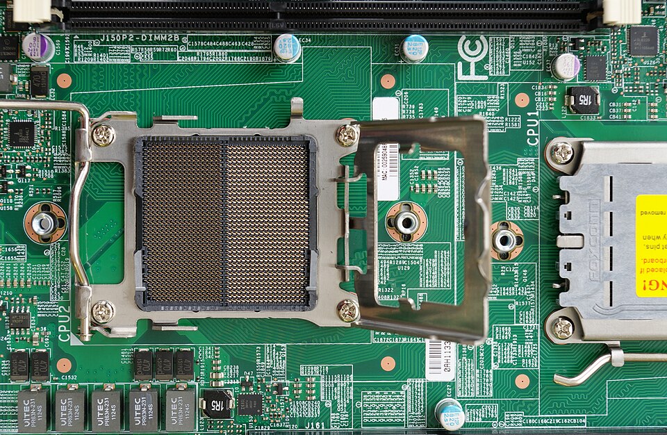 SAP-1’s architecture is implemented in real MPs like the 8085, which sits in a socket like this on a motherboard. (Image: smial (talk), FAL, via Wikimedia Commons)
Based on the TU BIT syllabus for Microprocessor and Computer Architecture (BIT151), unit 6.
Discussion
Loading…