Digital LogicUnit 59 min read
Flip-Flops, Latches & Sequential Logic Fundamentals
Unit 5 of Digital Logic covers sequential circuits' building blocks—SR, D, T, JK flip-flops, and latches—how they store state, their excitation tables, timing diagrams, and real-world applications in counters, registers, and memory. Master their truth tables, state transitions, and clocked vs. asynchronous behavior to
1. Sequential Circuits vs. Combinational Circuits
Sequential circuits remember past inputs (state) and produce outputs based on both current inputs and stored state. Unlike combinational circuits (e.g., adders, multiplexers), they have memory elements (flip-flops/latches) and timing constraints (clock signals).
flowchart LR
    A["Combinational Circuit"] -->|"No memory"| B["Output depends only on current inputs"]
    C["Sequential Circuit"] -->|"Has memory"| D["Output depends on current inputs + stored state"]
    D --> E["Flip-flops/Latches"]
    D --> F["Clock signal"]
Key difference:
| Feature | Combinational | Sequential |
|---|---|---|
| Memory | ❌ No | ✅ Yes (flip-flops) |
| Output dependency | Current inputs only | Current + past inputs |
| Timing | No clock required | Clock-driven |
| Example | Adder, MUX | Counter, Register |
2. Latches: Basic Memory Elements
Latches are level-sensitive (output changes when input level changes) and asynchronous (no clock). Two types:
A. SR Latch (Set-Reset)
- Inputs:
S(Set),R(Reset) - Outputs:
Q,Q̅(complement) - Forbidden state:
S=R=1(race condition → undefined output).
Truth Table:
| S | R | Q (next) | Q̅ (next) | State |
|---|---|---|---|---|
| 0 | 0 | Q | Q̅ | Hold |
| 0 | 1 | 0 | 1 | Reset |
| 1 | 0 | 1 | 0 | Set |
| 1 | 1 | ❌ | ❌ | Forbidden |
Circuit Diagram:
Worked Example: Design a latch to turn on a streetlight (Q=1) when a sensor (S=1) detects darkness, and turn it off (Q=0) when a switch (R=1) is pressed.
Solution:
- Use an SR latch with
Sconnected to the sensor andRto the switch. - Timing: Output changes immediately when
SorRchanges (no clock).
B. D Latch (Delay/Transparent Latch)
- Input:
D(data) - Output:
Q = DwhenEnable=1; holds lastDwhenEnable=0. - Used in: Data holding, transparent memory.
Truth Table:
| Enable | D | Q (next) |
|---|---|---|
| 0 | X | Q |
| 1 | 0 | 0 |
| 1 | 1 | 1 |
Circuit:
Real-World Tie-In:
eSewa’s Payment Verification
When you pay via eSewa, the system uses latches to hold your transaction data (D) until the bank confirms (Enable=1). Once confirmed, the latch updates (Q=1 for success) and holds the state until you log out.
3. Flip-Flops: Clocked Memory Elements
Flip-flops are edge-triggered (output changes only at clock edges) and synchronous (all flip-flops update simultaneously). Four types:
A. SR Flip-Flop
- Derived from SR latch but clocked.
- Forbidden state:
S=R=1at clock edge. - Uses: Simple state storage.
Characteristic Table (shows next state Q+):
| S | R | Q+ | Q̅+ |
|---|---|---|---|
| 0 | 0 | Q | Q̅ |
| 0 | 1 | 0 | 1 |
| 1 | 0 | 1 | 0 |
| 1 | 1 | ❌ | ❌ |
Excitation Table (shows required S, R for desired Q+):
| Q | Q+ | S | R |
|---|---|---|---|
| 0 | 0 | 0 | X |
| 0 | 1 | 1 | 0 |
| 1 | 0 | 0 | 1 |
| 1 | 1 | X | 0 |
B. D Flip-Flop
- Input:
D(data) - Output:
Q = Dat clock rising edge. - Advantage: No forbidden state; simpler design.
Truth Table:
| Clock | D | Q+ |
|---|---|---|
| ⏬ | X | Q |
| ⏫ | 0 | 0 |
| ⏫ | 1 | 1 |
Worked Example: Design a 1-bit register using a D flip-flop to store a bit from a sensor. Solution:
- Connect sensor output to
D. Qholds the last sensor value at each clock tick.
Real-World Tie-In:
Ncell’s Call Duration Counter
Ncell’s billing system uses D flip-flops to store call duration data (D) at each second (clock). The output Q accumulates the total duration for billing.
C. T Flip-Flop (Toggle)
- Input:
T(toggle) - Output:
Qtoggles (Q̅) whenT=1at clock edge. - Uses: Counters, frequency dividers.
Truth Table:
| T | Q+ |
|---|---|
| 0 | Q |
| 1 | Q̅ |
Worked Example: Design a toggle switch circuit for a traffic light. Solution:
- Use a T flip-flop with
T=1(always toggle). Qalternates between0(red) and1(green) at each clock pulse.
Timing Diagram:
D. JK Flip-Flop (Universal Flip-Flop)
- Inputs:
J(set),K(reset) - No forbidden state:
J=K=1→ toggle. - Most versatile: Can emulate SR, D, T flip-flops.
Characteristic Table:
| J | K | Q+ |
|---|---|---|
| 0 | 0 | Q |
| 0 | 1 | 0 |
| 1 | 0 | 1 |
| 1 | 1 | Q̅ |
Excitation Table:
| Q | Q+ | J | K |
|---|---|---|---|
| 0 | 0 | 0 | X |
| 0 | 1 | 1 | X |
| 1 | 0 | X | 1 |
| 1 | 1 | X | 0 |
Worked Example: Convert a JK flip-flop to a D flip-flop. Solution:
- Connect
J = D,K = Q̅(complement ofQ). - Now
Q+=Dat clock edge.
Real-World Tie-In: Khalti’s Transaction Lock Khalti uses JK flip-flops to lock transactions:
J=1(set) when a payment is initiated.K=1(reset) only after bank confirmation.J=K=1toggles the state if a timeout occurs (retry).
4. Flip-Flop Comparisons
| Flip-Flop | Inputs | Forbidden State | Uses |
|---|---|---|---|
| SR | S, R | S=R=1 | Basic memory |
| D | D | None | Registers, data storage |
| T | T | None | Counters, toggles |
| JK | J, K | None | Universal (emulates others) |
Advantages of JK over SR:
- No race condition.
- Can toggle (
J=K=1). - More flexible for design.
5. Master-Slave Flip-Flops
- Problem: Clock skew in single flip-flops.
- Solution: Master-slave configuration:
- Master captures input at clock rising edge.
- Slave outputs data at clock falling edge.
- Result: No glitches; stable output.
Circuit:
Timing Diagram:
Real-World Tie-In: Pathao’s Ride Allocation Pathao’s server uses master-slave flip-flops to allocate rides:
- Master: Captures rider request at clock tick.
- Slave: Assigns driver only after confirmation (falling edge).
6. Flip-Flop Applications
A. State Storage
- Example: Traffic light controller (red → green → yellow → repeat).
- Circuit: Use JK flip-flops with
J=K=1(toggle) and decode outputs for lights.
B. Counters
- Example: 4-bit binary counter using T flip-flops.
- Each flip-flop toggles when previous output is
1. - Timing Diagram:
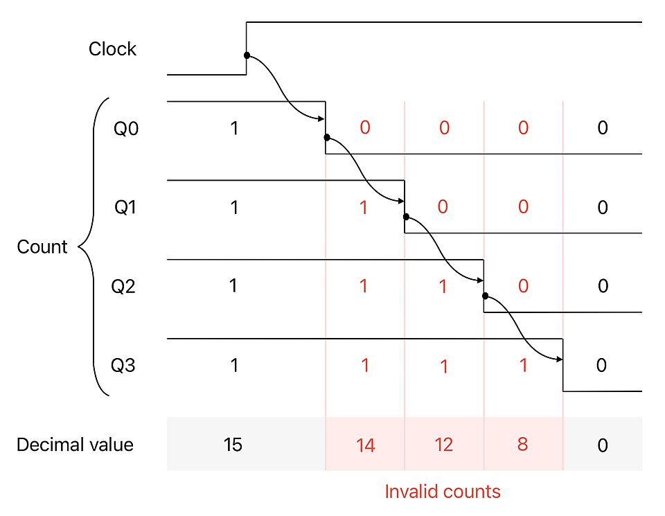 Q0-Q3 toggling sequentially. (Image: Lambtron, CC BY-SA 4.0, via Wikimedia Commons)
```
Q0-Q3 toggling sequentially. (Image: Lambtron, CC BY-SA 4.0, via Wikimedia Commons)
``` - Each flip-flop toggles when previous output is
Real-World Tie-In: NTC’s Electricity Meter NTC’s meters use flip-flop counters to track units consumed:
- Each pulse (from sensor) toggles a flip-flop.
- Output
Qaccumulates total units.
C. Registers
- Example: 8-bit register using D flip-flops.
- Each bit stored in a D flip-flop.
- Parallel load: All flip-flops update at same clock edge.
Circuit:
flowchart LR
    A["Clock"] --> B["D0"]
    A --> C["D1"]
    A --> D["D7"]
    B --> E["Q0"]
    C --> F["Q1"]
    D --> G["Q7"]
    E --> H["Output Bus"]
    F --> H
    G --> H
7. Asynchronous vs. Synchronous Flip-Flops
| Feature | Asynchronous (Latch) | Synchronous (Flip-Flop) |
|---|---|---|
| Trigger | Level-sensitive | Edge-triggered |
| Timing | Immediate output change | Output changes at clock edge |
| Power | Higher (always active) | Lower (clock-gated) |
| Use Case | Simple memory | High-speed counters/registers |
8. Exam Tip: How to Score Full Marks
Draw circuits correctly:
- Use standard gate symbols (no AND/OR symbols for flip-flops).
- Label clock, inputs, outputs, and states clearly.
- Example: For a JK flip-flop, show
J,K,CLK,Q,Q̅.
Show all tables:
- Characteristic table (next state).
- Excitation table (required inputs for desired state).
- Truth table (if combinational logic is involved).
Timing diagrams:
- Draw clock, inputs, and outputs on the same timeline.
- Mark rising/falling edges and state changes.
- Example: For a counter, show how outputs toggle.
Real-world connections:
- Link designs to eSewa (latches), Ncell (flip-flops), or NTC (counters).
- Example: "This JK flip-flop can be used in Khalti’s payment lock mechanism..."
Common pitfalls:
- Forgetting forbidden states in SR flip-flops.
- Misplacing clock edges in timing diagrams.
- Not showing feedback paths in sequential circuits.
Past Exam Question Analysis: Question: "Design a 2-bit asynchronous binary counter using T flip-flops." Expected Answer:
- Circuit:
- Two T flip-flops (
FF0,FF1). FF0.T = 1(always toggle).FF1.T = Q0(toggle only whenQ0=1).
- Two T flip-flops (
- Timing Diagram:
- Show
Q0,Q1toggling sequentially.
- Show
- State Table:
Q1 Q0 Next State 0 0 01 0 1 10 1 0 11 1 1 00
Real-World Tie-In: Daraz’s Order Queue Daraz’s order processing uses asynchronous counters (like this 2-bit design) to track pending orders:
- Each order toggles
FF0. - When
Q0=1andQ1=1, the system resets (order fulfilled).
Based on the TU BSc CSIT syllabus for Digital Logic (CSC116), unit 5.
Discussion
Loading…