PhysicsUnit 59 min read
Solid State Physics & Semiconductors: Band Theory, Doping, ICs & Devices
Unit 5 of Physics covers the atomic structure of solids, band theory of conductors/insulators/semiconductors, doping (n-type/p-type), semiconductor devices (diodes, transistors), fabrication (zone refining, ICs), and real-world applications in electronics and sensors.
1. Crystal Structure and Bonding in Solids
Key Concepts
- Crystal Lattice: Atoms/molecules arranged in a repeating 3D pattern (unit cell).
- Types of Bonding:
- Metallic: Free electrons (delocalized) → high conductivity (e.g., copper).
- Ionic: Strong electrostatic bonds (e.g., NaCl) → brittle, high melting point.
- Covalent: Shared electrons (e.g., diamond, silicon) → directional, strong.
- Van der Waals: Weak intermolecular forces (e.g., graphite layers).
Real-World Example: Silicon in Electronics
Silicon (Si) has a diamond cubic structure (covalent bonds), making it ideal for semiconductors. Its 4 valence electrons form stable bonds, but thermal energy can excite electrons to the conduction band → basis for all modern chips.
graph LR
    A["Crystal Structure"] --> B["Unit Cell"]
    B --> C["Bravais Lattice"]
    C --> D["Simple Cubic"]
    C --> E["Body-Centered Cubic"]
    C --> F["Face-Centered Cubic"]
    C --> G["Hexagonal Close-Packed"]
    G --> H["Silicon: Diamond Cubic"]
2. Band Theory of Solids
Energy Bands and Classification
| Material | Band Gap (Eg) | Conductivity | Example |
|---|---|---|---|
| Conductor | 0 eV | High (overlap) | Copper, Aluminum |
| Semiconductor | 0.1–4 eV | Moderate (temperature-dependent) | Silicon (1.1 eV), Germanium (0.7 eV) |
| Insulator | >4 eV | Very low | Diamond, Rubber |
- Valence Band (VB): Filled with electrons at 0 K.
- Conduction Band (CB): Empty at 0 K; electrons here can move freely.
- Band Gap (Eg): Energy difference between VB and CB.
- Intrinsic Semiconductors: Pure Si/Ge (Eg ~1 eV). Conductivity increases with temperature (more electron-hole pairs).
- Extrinsic Semiconductors: Doped with impurities (e.g., P in Si → n-type; B in Si → p-type).
Worked Example: Silicon’s Band Gap
At room temperature (300 K), the intrinsic carrier concentration for Si is . Calculate the band gap using: Where:
- : Effective density of states (~).
- : Boltzmann constant ().
- .
Solution:
3. Doping and Semiconductor Types
Doping Process
- n-type: Add pentavalent impurities (e.g., P, As) → extra electron → majority carriers = electrons.
- p-type: Add trivalent impurities (e.g., B, Al) → "hole" (missing electron) → majority carriers = holes.
Carrier Concentration
For an n-type semiconductor: For a p-type semiconductor: Where = donor concentration, = acceptor concentration.
Real-World Example: Solar Panels (eSewa’s Home Systems)
Solar cells use p-n junctions (Si doped with B and P). When sunlight excites electrons in the depletion region, they move to the n-side, creating a voltage → electricity.
sequenceDiagram
    participant Sunlight
    participant p-type
    participant n-type
    participant Circuit
    Sunlight->>p-type: Photon absorption
    p-type->>n-type: Electron-hole pair generation
    n-type->>Circuit: Electron flow (current)
    Circuit->>Load: Power delivery
4. Semiconductor Devices
a) p-n Junction Diode
- Forward Bias: Reduces barrier → current flows (e.g., LEDs, rectifiers).
- Reverse Bias: Increases barrier → negligible current (until breakdown).
- Applications:
- eSewa’s Smart Meters: Use diodes to measure AC current direction.
- Khalti’s Payment Systems: Diodes in voltage regulators for stable power.
b) Bipolar Junction Transistor (BJT)
- Structure: n-p-n or p-n-p.
- Operation: Current through base controls collector-emitter current.
- Example: Used in Ncell’s base stations for signal amplification.
 Shows emitter, base, collector, and current directions. (Image: Osbert Joel for Electrical Classroom, CC BY-SA 4.0, via Wikimedia Commons)
c) Field-Effect Transistor (FET)
- MOSFET: Metal-Oxide-Semiconductor FET (used in all modern chips).
- Operation: Gate voltage controls channel conductivity.
- Example: Daraz’s servers use MOSFETs for low-power logic circuits.
5. Semiconductor Fabrication
Purification: Zone Refining
- Impure Si is melted in a narrow zone; impurities move to one end → 99.9999999% purity.
- Example: Used to make single-crystal Si ingots for chips.
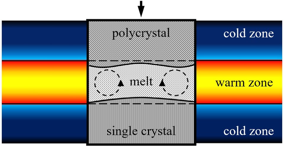 Shows molten zone moving through a Si rod. (Image: Dbuckingham42, CC BY-SA 4.0, via Wikimedia Commons)
Single Crystal Growth (Czochralski Method)
- A seed crystal is dipped into molten Si and slowly pulled → large single crystal.
- Example: Intel/AMD processors start as single-crystal wafers.
IC Fabrication Steps
- Wafer Preparation: Thin Si slices (0.5–1 mm).
- Oxidation: Grow SiO₂ layer (insulator).
- Photolithography: Pattern circuits using UV light.
- Doping: Ion implantation for n/p regions.
- Metallization: Add aluminum/copper for connections.
6. Electrical Conductivity of Semiconductors
Intrinsic Conductivity
Where:
- : Intrinsic carrier concentration.
- : Electron/hole mobility (~1500 cm²/V·s for Si).
Extrinsic Conductivity (Doped)
For n-type: For p-type:
Temperature Dependence
- Intrinsic: → increases with T.
- Extrinsic: (at low T, carriers freeze out).
7. Applications in Nepal
| Company/Product | Semiconductor Concept Used | How It Works |
|---|---|---|
| eSewa | p-n Junction Diodes | Rectifies AC to DC for smart meters. |
| Khalti | MOSFETs in Voltage Regulators | Stabilizes power for payment terminals. |
| Ncell | BJTs in Amplifiers | Boosts signal strength in base stations. |
| NTC (Electricity Board) | Semiconductor Relays | Automates grid switching. |
| Pathao | CMOS Logic (Microcontrollers) | Processes GPS/ride data in driver apps. |
Exam Tip
- Band Theory: Always draw VB/CB diagrams for conductors/insulators/semiconductors. Memorize Eg values for Si (1.1 eV) and Ge (0.7 eV).
- Doping: For n-type, ; for p-type, . Assume full ionization unless stated.
- Devices: Know the symbols for diodes, BJTs, and MOSFETs. Explain forward/reverse bias with current directions.
- Fabrication: Zone refining → single crystal → photolithography → doping. Link to real chips (e.g., "This is how your phone’s processor is made").
- Graphs: Plot vs for intrinsic/extrinsic semiconductors. Label axes and trends.
- Numerical Problems:
- Calculate or using .
- Find conductivity given or .
Key Formula Summary:
| Concept | Formula |
|---|---|
| Intrinsic carrier conc. | |
| n-type conductivity | |
| p-type conductivity | |
| Band gap (from ) |
Based on the TU BSc CSIT syllabus for Physics (PHY118), unit 5.
Discussion
Loading…